Thus, the authors created the cavity that confined the photons within eight-nanometer silicon bridges with an ultra-high aspect ratio of 30 to perform the first empirical illustration of photon containment to a single hotspot just below the diffraction limit in dielectrics. The suggested framework ushered in a new era of subtractive manufacturing and high-performance additive through topology optimization and fabrication integration.
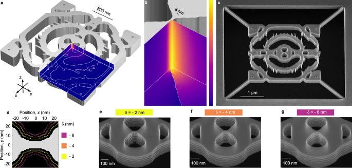
Fabrication of topology-optimized silicon dielectric bowtie cavity (DBC). a Rendering of the DBC design generated by tolerance-constrained topology optimization. The normalized ∣E∣-field is projected on the faces defining the three symmetry planes of the design. b Zoom-in of the solid silicon bowtie exhibiting a strong field confinement due to the bowtie bridge dimension of 8 nm. c 40° tilted scanning electron microscopy (SEM) image of a fabricated cavity. d Global geometry-tuning, δ. Each air (black) pixel (1 nm2) inside a δ-outline is exposed uniformly with electron-beam lithography; hence, air features defining the device are uniformly tuned. e–g 40° tilted SEM images of bowtie region for δ = { − 2, − 4, − 6} nm. We measure the mean width of the fabricated bowties to be (8 ± 5) nm, (10 ± 5) nm, and (16 ± 5) nm for figures e, f, and g, respectively, noting the variation in width along the z-direction caused by the scallops and ~1° negative sidewall angle represented by the uncertainty as discussed in the main text. Image Credit: Albrechtsen, M et al., Nature Communications
Understanding Photon Confinement in Optical Nanocavities
Storing and confining light in optical nanocavities is necessary to enhance the interaction between electrons and photons in a semiconductor instrument. Various methods can create nanocavities, such as topological confinement, distributed Bragg reflection, Fano resonance or bound states in the continuum, and total internal reflection.
These methods have improved the temporal confinement orders of magnitude, but none of them support optical mode volume (V) in the deep subwavelength zone. Alternatively, metal nanoparticle plasmons can restrict light to the diffraction limit, but the quality factors are severely constrained by the metal's absorption losses, which are considerably below 100.
In this work, the authors also considered lossless dielectrics. Still, to maximize the light-matter interaction in the design's focal point, they applied topology optimization instead of geometry optimization of a design based on human perception. Prior theoretical studies discovered that this process produced dielectric bowtie cavities (DBCs).
However, more current theoretical studies noted that inverse design was prone to create unrealistic designs unless restrained by the restrictions of materials and production. Thus, to build a compact nanocavity, the fabrication restrictions of a cutting-edge nanofabrication technique were first measured. Then, these constraints were directly used in the topology optimization.
This fusion of design and manufacture yielded an innovative and realistic cavity. Even though lithography-based nanotechnology was particularly well suited to precisely map designs onto fabricated devices, achieving fabrication-restrained topology-optimized devices was a tremendous challenge in inverse design.
According to Marcus Albrechtsen, PhD-student at the Technical University of Denmark (Electro) and the first author of the novel research, “Although computer calculations show that you can concentrate light at an infinitely small point, this only applies in theory. The actual results are limited by how small details can be made, for example, on a microchip.”
Far-field spectroscopy and scanning electron microscopy (SEM) were used to achieve a consistent image of theory and observation for structural and spectral features. Finally, near-field spectroscopy established an upper bound for the experimentally realized mode volume below the diffraction limit. Therefore, this study was the first experimental proof of the confinement of light in dielectric cavities below the diffraction limit.
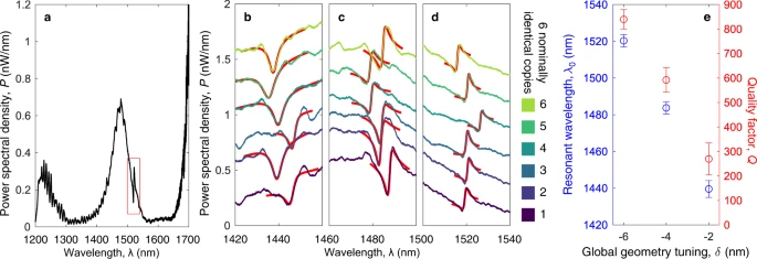
Optical far-field characterization of dielectric bowtie cavities. a Broadband spectrum of a cavity with δ = − 6 nm. The cavity mode interferes with a background mode yielding a Fano resonance centered at λ ~ 1520 nm, highlighted by the red box. b–d Spectra for six nominally identical devices for each tuning δ = { − 2, − 4, − 6} nm. The spectrum of each copy is offset incrementally by 0.25 nW nm−1 for clarity. The full spectrum for cavity 5 is shown in a. The red lines show fits to the Fano lineshape. e Mean and standard deviation of resonant wavelength λ0 (blue, left) and quality factor Q (red, right) against δ, extracted from the fits in b–d. Image Credit: Albrechtsen, M et al., Nature Communications
Proof-of-Concept Investigations
Maxwell's equations were applied in a finite volume of space to simulate the physics for the inverse design process, assuming time-harmonic field behavior. Also, using symmetry criteria and first-order absorption boundary conditions, the authors used the DBC structure's three-fold spatial symmetry to condense the model and truncate the modeling domain.
A silicon-on-insulator wafer having a 240-nanometer (100) device layer and a three-micrometer buried oxide was cut into a 25 by 25-millimeter chip. It was initially cleaned with acetone, followed by deionized water and isopropanol (IPA), and dried with dry nitrogen (N2). Finally, the size of the manufactured structures was determined by contrasting top-view and slanted SEM images that underwent in-depth image analysis.
The predicted local density of optical states (LDOS) in the domain's geometric center, which was required to be solid, was maximized using measured manufacturing limitations as input to size- and tolerance-restrained topology optimization. As a result, the optimization was shielded from surface-level local lightning-rod effects and achieved robust confinement within the dielectric bowtie.
Thus, the findings showed that by adjusting the material layout in a tiny square area with a side length of 2ë, the topology optimization aimed for a maximum LDOS of about 1550 nanometers. The proposed DBC fabrication was based on these criteria, and the produced structures exhibited agreement with the desired geometry.
Although the findings clearly showed photon confinement well below the diffraction limit, the modes were so compact that the authors could not determine their exact size. Therefore, for a thorough comparison of theory and experiment for DBCs, measuring the width of the manufactured silicon bridge was essential.
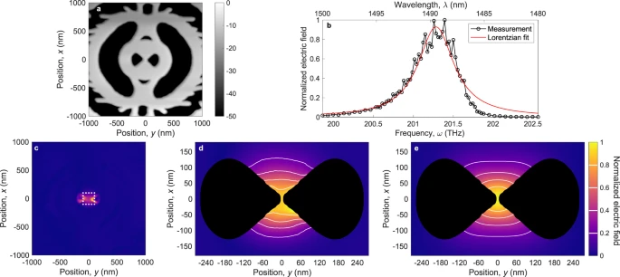
Scattering-type scanning near-field optical microscopy (s-SNOM) of cavity mode. a Topography measured by atomic force microscopy (AFM). b Spectrum measured of amplitude of scattered field with Lorentzian fit, λ0 = (1489.4 ± 0.1) nm and Q = 370 ± 40. c s-SNOM signal on resonance demonstrating strong field localization with excellent suppression of background noise. The white dotted box highlights a square domain with its side length given by the diffraction limit, λ0/(2nSi) ~ 200 nm. The strong signal in the cavity voids arises due to complex interactions between the AFM probe and the cavity mode. d Normalized measured amplitude of the light scattered from the cavity surface with the voids blacked out. e Numerical simulation of experiment, ff(σ = 37 nm) ∗∣Ec∣2, confirming photon localization below the instrument response function as explained in the main text. The s-SNOM measurements presented here were performed on cavity copy 3 (δ = − 4 nm), which has a mean bowtie width of 10 nm. Image Credit: Albrechtsen, M et al., Nature Communications
Significance of the Study
This research offered the first demonstration of the merits of topology optimization with measurable fabrication restrictions. Thus, the findings established a new benchmark for photonic nanotechnology in searching globally optimum structures. Also, the study showed photon confinement within dielectrics for the first time below the diffraction limits without inherent Q restrictions.
Directly enhanced light-matter interaction in the proposed cavity was increased by a Purcell factor of 6 x 10³ across a bandwidth of two nanometers owing to the directly adjusted LDOS of the cavity. Due to the small device footprint of 4ë2, this wide bandwidth was incorporated in the cavity design and was required for nonlinear optics, and optical interconnects.
Direct studies of broadband Purcell factors might be possible with the proposed cavity and embedded emitters. This work demonstrated previously unseen levels of photon confinement within dielectrics. Also, it paved the way for studies in extreme regimes of light-matter interaction, which could suppress quantum decoherence caused by phonons.
By extending the design domain, the authors achieved a much higher Q. In most fields of semiconductor nanotechnology, notably nanophotonics, nanoelectromechanics, cavity optomechanics, and quantum photonics, experimental domains were opened by the capacity to construct highly tailored devices with eight-nanometer dimensions and high aspect ratios.
Reference
Albrechtsen, M et al. (2022). Nanometer-scale photon confinement in topology-optimized dielectric cavities. Nature Communications. https://www.nature.com/articles/s41467-022-33874-w
Disclaimer: The views expressed here are those of the author expressed in their private capacity and do not necessarily represent the views of AZoM.com Limited T/A AZoNetwork the owner and operator of this website. This disclaimer forms part of the Terms and conditions of use of this website.