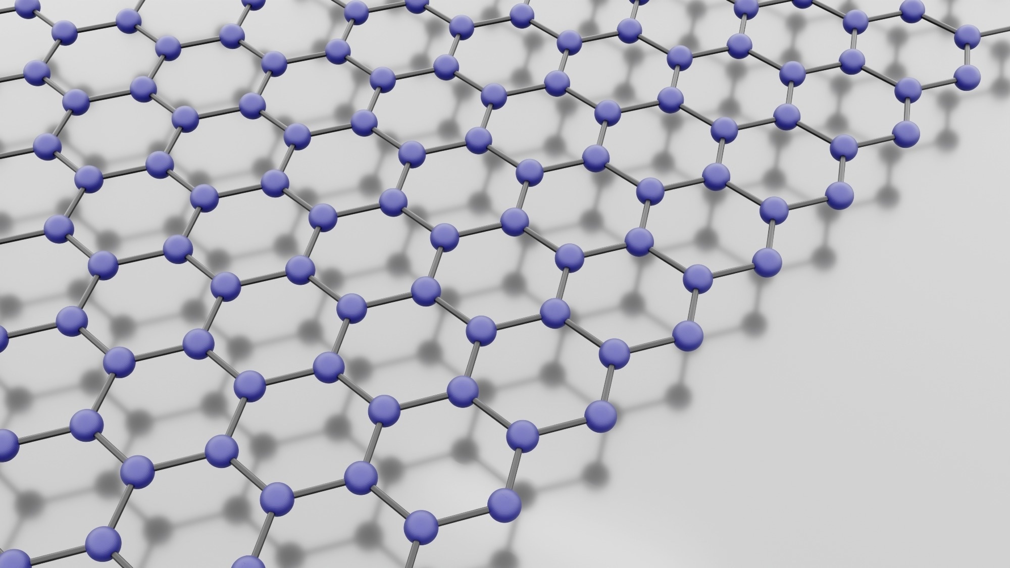
In a study recently published in npj 2D Materials & Applications, researchers explored whether the mineral vermiculite can be processed into atomically thin nanosheets with both semiconducting behavior and antiferromagnetic properties, specifically those with wide band gaps and antiferromagnetic order.

Image Credit: MZinchenko/Shutterstock.com
Background
As the demand grows for scalable, cost-effective, and eco-conscious materials in next-generation electronics and photonics, two-dimensional (2D) materials have become a major area of focus.
Vermiculite, a phyllosilicate mineral, is especially interesting due to its layered 2:1 silicate structure, which allows it to swell and separate into individual sheets. These layers consist of negatively charged silicon-oxygen tetrahedra and positively charged interlayer cations, which vary in composition.
Depending on whether the octahedral layers are filled with ions like magnesium (Mg), aluminum (Al), or iron (Fe), the mineral can be dioctahedral or trioctahedral. Interlayer cations such as potassium (K+), magnesium (Mg2+), or sodium (Na+) influence the mineral’s swelling and delamination behavior.
The Current Study
The research team set out to exfoliate vermiculite into single-layer nanosheets using a combination of chemical and mechanical methods, then characterize their physical, electronic, and magnetic properties.
Natural vermiculite samples were sourced from various regions, acknowledging that natural compositional differences could impact both the delamination process and the nanosheets’ final properties.
To prepare the mineral for exfoliation, K+ ions in the interlayer spaces were exchanged with Na+ ions. This ion exchange reduced electrostatic forces, making it easier to separate the layers during the next steps.
Chemical exfoliation was carried out using solvents such as dimethyl sulfoxide (DMSO), dimethylformamide (DMF), and N-methyl formamide (NMF). The solvents’ ability to penetrate between layers and promote swelling proved critical.
After immersion, the samples underwent sonication, which broke down the bulk material into thin, individual nanosheets. Researchers fine-tuned variables like solvent type, sonication time, and ion exchange conditions to optimize yield and sheet quality.
Advanced characterization techniques were used to analyze the resulting nanosheets. Atomic force microscopy (AFM) measured sheet thickness and lateral size, while X-ray diffraction (XRD) and synchrotron-based methods confirmed structural integrity and exfoliation.
X-ray photoelectron spectroscopy (XPS) examined surface chemistry and elemental composition. Magnetic properties were assessed using Mössbauer spectroscopy, and electronic structure predictions were supported by density functional theory (DFT) simulations.
Results and Discussion
Using this combined chemical-mechanical process, the team successfully exfoliated vermiculite into monolayer nanosheets approximately 0.95 nm thick. Replacing K+ with Na+ significantly improved swelling and delamination. Among the solvents tested, DMSO, DMF, and NMF were the most effective, enabling consistent exfoliation into high-aspect-ratio sheets.
XPS results confirmed successful ion exchange and retention of the silicate framework. Synchrotron XRD revealed broader peaks typical of exfoliated structures, while maintaining the crystalline order of the material.
Electronic measurements showed that the nanosheets are wide band-gap semiconductors, with energy gaps between 3.3 and 3.9 eV—well-suited for high-power and high-frequency applications, and wider than those of many traditional semiconductors. Mössbauer spectroscopy detected antiferromagnetic ordering within the sheets, a desirable property for spintronic devices. The magnetic behavior was linked to the arrangement of metal cations in the octahedral layers, a feature preserved even after exfoliation.
DFT simulations further suggested that substituting different elements, such as iron or aluminum, could be used to tune the electronic and magnetic characteristics. The results demonstrate that vermiculite nanosheets can be produced in large quantities without structural defects, making them viable for advanced electronic applications.
Download your PDF copy now!
Conclusion
This study presents vermiculite as a promising, sustainable material for producing 2D semiconductors. Naturally abundant, low-cost, and environmentally safe, it offers a compelling platform for developing next-generation electronic and spintronic devices. Its ability to be chemically modified and mechanically processed into high-quality nanosheets adds to its appeal for scalable applications.
While the findings are encouraging, the researchers emphasize the need for continued work. Future studies should aim to refine delamination techniques, better control the mineral’s compositional variations, and explore how structural imperfections affect performance.
We also need to test how these nanosheets behave in real-world conditions and integrate them into devices using scalable, industry-compatible fabrication methods.
Journal Reference
Pacakova B., et al. (2025). Naturally occurring 2D semiconductor with antiferromagnetic ground state. npj 2D Materials & Applications. DOI: 10.1038/s41699-025-00561-5, https://www.nature.com/articles/s41699-025-00561-5