Nov 28 2007
Researchers at the National Institute of Standards and Technology (NIST) have demonstrated a mechanical fatigue process that eventually leads to cracks and breakdown in bulk silicon crystals—a phenomenon that’s particularly interesting because it long has been thought not to exist. Their recently published results have important implications for the design of new silicon-based micro-electromechanical system (MEMS) devices that have been proposed for a wide variety of uses.
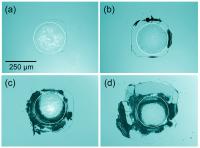 Optical micrographs of contact damage in silicon from cyclic stress show progressive damage after (a) 1,000 cycles, (b) 5,000 cycles, (c) 20,000 cycles and (d) 85,000 cycles. Color added for clarity, white circle shows computed size of the contact circle.
Silicon - the backbone of the semiconductor industry - is one the world’s most heavily studied materials, and it has long been believed to be immune to fatigue from cyclic stresses because of the nature of its crystal structure and chemical bonds. And indeed, conventional tests have validated this. Recent research into silicon MEMS devices, however, has revealed that these microscopic systems that incorporate tiny gears, vibrating reeds and other mechanical features do seem to develop stress-induced cracks that can lead to failure. Why this happens at the microscopic scale is a matter of debate. One school of thought holds that the effect is purely mechanical, due to friction, and the other argues that it essentially is caused by corrosion - a chemical effect. Because the effect has only been noticed at submicrometer scales, it has been difficult to determine which theory is correct.
A material’s resistance to cracking - referred to as “toughness” by materials scientists - is measured customarily by taking a sample of the material, slightly notching one edge, and pulling on the ends repetitively to see if the tensile stress causes the notch to grow into a crack. Bulk silicon always has passed this test. But, argued the NIST team, in real-world MEMS devices the stresses are likely to be much more complicated.
To test this, they used an alternate method: pressing the top of test crystals with tiny tungsten-carbide spheres about 3 mm in diameter at pressures below the silicon’s breaking point. Simply pressing down hard on the crystal for days at a time caused no detectable cracks—arguing against the corrosion theory. On the other hand, using half the pressure but cycling the test hundreds of thousands of times revealed a gradually increasing pattern of surface damage at the indentation site—clear indication of mechanical fatigue. The NIST team, which included a researcher from the University of Extremadura in Spain, theorizes that the critical element in their experiments is the addition of shear stress (causing the crystal planes to slide against each other), a component missing in conventional tensile strength tests but not uncommon in real-world applications.
The NIST experiments demonstrated fatigue effects in silicon at the comparatively large scale of hundred of micrometers. The next step is to determine if the same mechanisms operate at the submicrometer level.