Jan 16 2008
Nanowires and nanolayers are at the forefront of advanced electronics, photonic and sensor research. Of paramount importance to researchers are the tools to produce such materials. Structured Materials Industries Inc. announces the delivery of the largest such reactor to date - designed to produce nanowire and nanolayer films on wafers up to 8” in diameter. The tool features multiple operating modes including rapid heating to > 950°C as well as sustained heating at temperature.
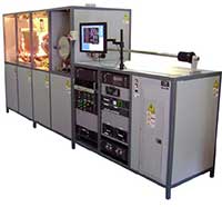 NanoWire and NanoLayer growth tool
Features of the tool include fully automated growth control of several process chemical sources with multiple safety interlocks, high temperature operation from low pressures to atmospheric pressure, and data/trend recording - all housed in a paneled all-welded steel frame.
This advanced design tool is expected to help advance nanomaterials research.