Graphene, the wonder material, is the subject of most researchers and comprises of carbon atoms that form angstrom-thick two-dimensional sheets. These sheets can be seen as multi-layers in graphene flakes. To this end, non-destructive measuring tools are required to determine the properties of graphene. One such tool is Confocal Raman-AFM, which is effective for studying nanomaterials. Integration of confocal Raman microscopy and AFM enables the high spatial and topographical resolution obtained with an AFM to be directly linked to the molecular data rendered by confocal Raman spectroscopy.
Two examples are presented to underline the power of the alpha300 RA confocal Raman-AFM microscope system for the non-destructive characterization of graphene.
The Methods
In Raman imaging, the Raman spectra are obtained with a combination of high-throughput confocal microscope and Raman spectrometer. Atomic force microscopy (AFM) offers spatial data parallel and perpendicular to the surface with resolution in the nanometer range. Along with topographic high resolution information, local material properties such as stiffness and adhesion can be studied by analyzing the interaction forces between the tip and sample. The combination of confocal Raman microscopy with AFM is a significant advancement in microscopy.
Example Measurements: Exfoliated Graphene
Imaging of Multilayered Graphene
Figure 1 depicts the white light image (a), the AFM topography image (b), and the Raman image (c) of a graphene flake, all obtained with an alpha300 RA microscope, without manually moving or shifting the sample between different measurements. Through exfoliation, the graphene flake was deposited on the oxide top layer of a Si-wafer.
The white light image as shown in Figure 1a helps in the coarse examination of the Si-wafer following deposition of graphene. The alpha300 RA has precise cantilever positioning capabilities and thus enables AFM imaging of the same graphene flake. The 3D-physical dimensions of the graphene flake are shown on the AFM topography image in Figure 1b. The black line in (b) signifies the cross section of a height profile.
The Raman Image as shown in Figure 1c was studied from a 2D spectral array, consisting of 150 x 150 Raman spectra. For each Raman spectrum in the 2D spectral array, the integration time was 0.05s per spectrum, resulting in a total acquisition time of less than 20 minutes.
The typical Raman spectra for a mono-bi-, and multi-layer of graphene are shown in Figure 1e; the unique D, G, and G' Raman bands of carbon nanomaterials are also shown. These spectra were utilized as the base spectra for the basis analysis software tool applied in the WITec Project software. The color coded Raman image in Figure 1c was produced using this algorithm. The spectral colors as shown in Figure 1e are identical to the colors in the Raman image shown in Figure 1c.
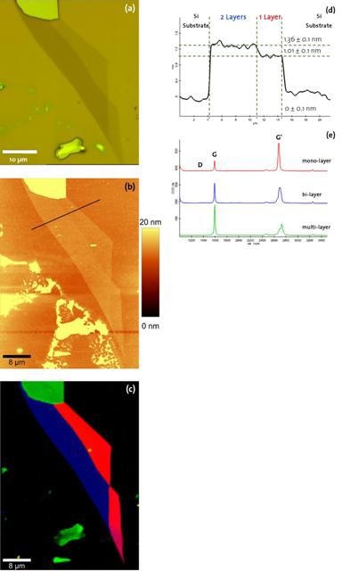
Figure 1. (a) White light image of a graphene flake on a silicon surface. (b) AFM topography image (AC-mode) of graphene, (c) Color coded Raman image. (d) Height profile along the cross section indicated in Fig. 1b (black line). (e) Raman spectra measured at different positions of the graphene flake (colors correspond to Fig. 1c).
Analysis of Raman Bands of Carbon Nano-Materials Using WITec Software
The WITec data analysis software offers algorithms that are useful for a comprehensive analysis of 2D Raman spectral arrays. As reported in the papers published on data acquired with a WITec alpha300 R microscope, graphene's Raman spectra offer accurate information on the phonon energy dispersion, electronic band structure, crystal structure, and the electron-phonon interaction in sp2 carbon systems. It is possible to probe the defects, doping, crystal orientation, thermal conductivity, linear dispersion of electronic energy, strain and the number of layers by monitoring the width, position, line shape and integrated intensity of the Raman features of the graphene layers.
The G and G’ bands are the most prominent peaks in the Raman spectrum of graphene which are related to the double degenerate in the plane transverse optical phonon (iTO) and longitudinal optical phonon modes (LO). G band intensity is directly proportional to the number of graphene layers and is thus a measure for the number of layers in a graphene flake. A Lorenzian curve is fitted to the G band, a shift towards lower wave numbers is seen with an increase of graphene layer numbers, as shown in Figure 2.
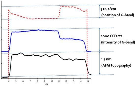
Figure 2. Variations in G-band position and G-band intensity in comparison with the height profile of the AFM topography image.
In the case of exfoliated graphene monolayer as in Figure 3a, the G' band is defined by a single Lorenzian fit, while in the case of bilayer and multi-layer as shown in Figure 3b and 3c, four Lorenzian curves are required revealing the interplane phonon interaction.
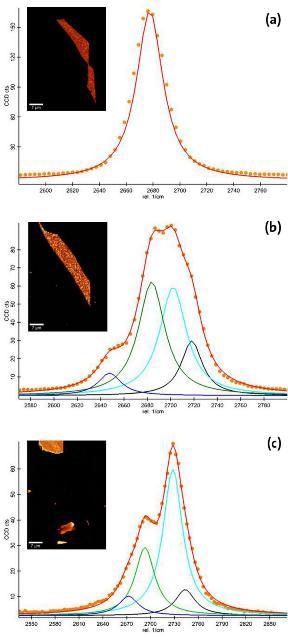
Figure 3. Line shape of the G'-band and Lorenzian fit of the 2D spectral array for (a) monolayer, (b) bi-layer, (c) multi-layer of graphene.
Chirality Investigations of Graphene
In case some defects are present at graphene edges, an additional peak will appear in the Raman spectrum of graphene termed a D-band, which is due to an intervalley double resonance process involving iTO phonons and defects. Figure 4a illustrates the integrated intensity of the D-band along the cross-section marked in Figure 1b along with the height profile from the AFM topography image. Figure 4b shows the corresponding Raman spectra from the graphene flake edges with highlighted D-band.
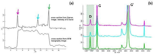
Figure 4. (a) Comparison of D-band intensities with the height profile along the cross-section indicated in Fig 1b. (b) Raman spectra from the positions marked in Figure 4a.
Edge angles as multiples of 30° are present in most of the graphene flakes. An edge angle of 30°, 90° or 150° degree denotes different chiralities (armchair or zigzag) between two adjacent edges; whereas, edges with angles of 60° or 120° exhibit the same chirality as shown in Figure 5a. These findings underline the potential of the confocal Raman-AFM in the design and characterization of new optoelectronic devices, based on the unique optical, magnetic, and superconductive properties of graphene edges.
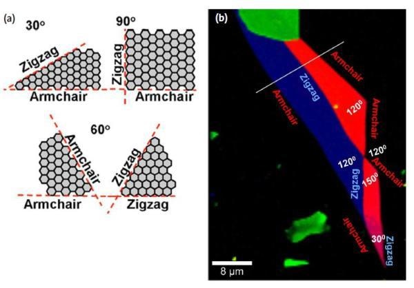
Figure 5. a. Examples of graphene layer angles and their corresponding chiralities (zigzag or armchair, according to You et al., 2008). (b) Determination of the edge chirality (zigzag or armchair) through evaluation of the D-band intensity and comparison with the angles of the different graphene layers.
Applications of graphene-based devices, using its excellent phononic and electronic properties, require techniques to form uniform single layer graphene films on dielectric substrates on a large scale.
Figure 6 depicts a confocal Raman AFM study of a CVD graphene layer deposited on an Si substrate. An area of 10x10µm2 was scanned in both Raman and AFM AC imaging mode.
By comparing the high resolution AFM image as shown in Figure 6a with the color coded Raman image as shown in Figure 6c, the two graphene domains with wrinkles imaged with the AFM can be clearly seen in the Raman image as they are enclosed by the defected structure. The high resolution topographic structures can be clearly linked to the observed spectral features (see white arrows).
Figure 6. Defects in graphene layers (a) 5 x 5pm2 AFM topography image, topography range: 0-10nm. (b) AFM and Raman image overlaid (c) 10 x 10µm2 Raman image of the same sample area as shown in (a) with lower magnification.
Conclusion
Thus, the combination of confocal Raman and AFM microscope system can be used for the non-destructive characterization of graphene.

This information has been sourced, reviewed and adapted from materials provided by WITec GmbH.
For more information on this source, please visit WITec GmbH.