Scientific research, medical imaging, and safety monitoring have used X-rays in the past and continue to do so in the present. Since the introduction of X-rays, radiation sensing has been a topic of ongoing research; several materials are continuously developed for detecting high-performance nanoparticles.

Image Credit: Roberto Lo Savio/Shutterstock.com
Generally, the wavelength of observable light ranges from 400 to 700 nm in the visible spectrum. X-rays considered high energy have wavelengths of less than 0.0110 nm (100,000 eV), which are invisible to humans. Currently, the methods for detecting high energy radiations are in great demand, due to which the development of new methods is essential. Some of the traditional methods include X-ray films, phosphor-based detectors, semiconductor-based detectors, and gas detectors.
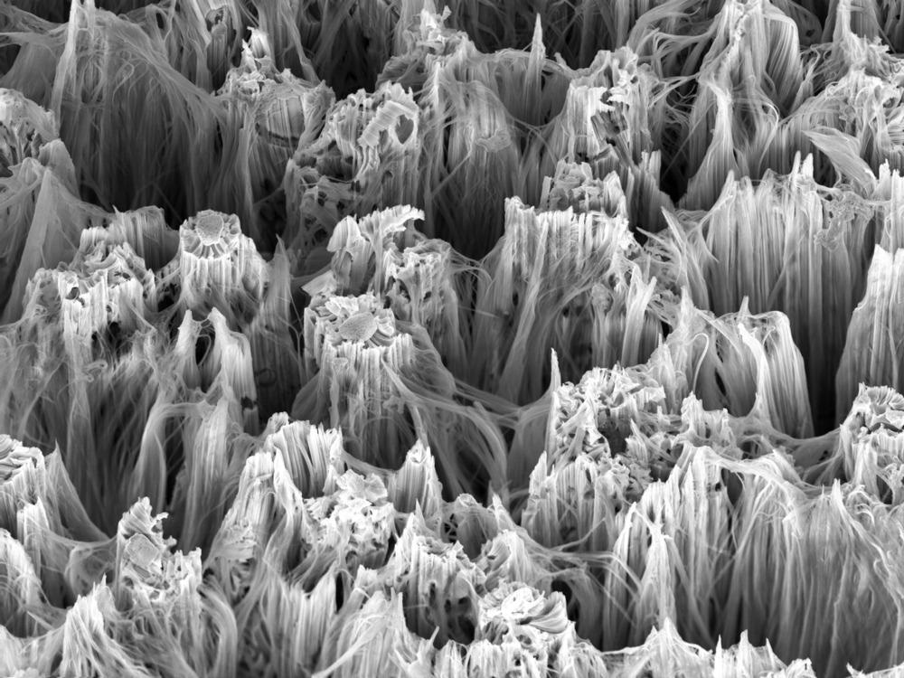
The prospect of semiconductor nanowires (NWs) as an essential part of nanoscale devices and electronic circuits has sparked much research in the last decade or so. Three distinct features of NWs have fuelled previous investigations. First, they demonstrate laser guiding and electronic driving capabilities simultaneously.
Secondly, their high specific surface area ratio improves their contact with the environment, making them very sensitive. The elastic deformation relaxation at the outer surface also enables the construction of new heterostructures that are not possible in planar geometry. Lastly, their properties are substantially influenced by their orientation, making them suitable for use as polarization-dependent sensors.
Nano Size Effects
The materials used in X-ray imaging can be prepared as nanoparticles, nanocomposites or transparent nanoceramics. Using these materials in x-ray imaging has different effects; some of them are discussed below:
Quantum Confinement Effect
Quant confinement occurs when a particle's dimensions are decreased to the nanoscale due to a drastic decrease in quantum mechanical permitted phases in tiny particles, resulting in higher bandgap energy. The optical properties, luminescence endurance, and quantum efficiency of emission are all affected by this phenomenon.
Surface Effect
Relative to the bigger-sized materials, nanoparticles have a greater area ratio. Because the greater surface area frequently contains quenched centers, surface modification is necessary. The Core-shell system is one of the techniques used for that purpose.
Structural Effect
Surface tension may cause structural deformation of crystalline structure when the dimensions of the materials are reduced to the nanoscale. Moreover, compared to big volume bulk voids, crystallinity and the number of structural flaws are decreased inside a tiny volume of nanoparticles.
Role of Nanowires
Most NW approaches depend on the capacity to describe individual and groups of NWs structurally, optically, and electrically. At the same time, singular probes that address all of these attributes concurrently are rare to come by.
Using synchrotron-based sensors in the cross-energy spectrum has a lot of potential and offers a variety of benefits, including ground knowledge depths, element and orbital specificity, and instantaneous availability to K absorption edges and X-ray fluorescence emission paths of hard, moderate, and light elements.
As a result, current synchrotron types of radiation, like X-ray microdiffraction techniques, have played a significant role in the rapid evolution of nanowire technology. Furthermore, lens-less techniques have been used to analyze ZnO NWs using Bragg coherent diffraction imaging.
The capability to track the full stress tensor in 3D with the nanometric precision resolution has the potential to be extremely useful for studying complicated nanostructures. Still, there are a few major drawbacks in this case, due to which the information related to NWs occurrences is limited.
The majority of synchrotron processes are now conducted out in arrays of NWs, with data acquired through spatial averaging at huge large scales. As a result, for three reasons, adding nanometric spatial resolving capabilities to X-ray imaging in NW investigations is widely desired:
First, the utilization of strong X-ray pencil nanobeams is required to analyze small embedded zones with signal attenuation and complex structures. Secondly, thanks to the excellent clarity and low transmissivity of today's third-generation synchrotron sources, it is now viable to center X-rays to spot sizes tinier than nanowires using a variety of focusing devices like Fresnel zone plates and Kirkpatrick-Baez mirrors.
Lastly, because of the multiple photon-matter linkages, these X-ray nanoprobes can be used for a range of applications in NWs, including super sensitive elemental testing using XRF/XAS, minority phase recognition, and strain fields by XRD sin nanoscale precision.
The chemical characteristics, measurements, and strain dispersion of core-shell NWs using grazing occurrence, as well as the dynamics and interactions of the tension M1–M2 structural phase transformation in each nanowire, the native framework of single semiconductor, wrapped nanotubes, the chemical characteristics, measurements, and strain dispersion of core-shell NWs, are all instances of using X-ray microbeams to preserve spatially resolved properties of single NWs
Overall, the usage of nanomaterials for X-ray detection is limited compared to other nanomaterial applications. Excitation methods, novel scintillator materials, and actual chemical applications are all involved in research on X-ray detection using nanomaterials.
Continue reading: How Can Nanocrystal Size Affect X-Ray Diffraction Results?
References and Further Reading
Cole, M. T., Parmee, R. J., & Milne, W. I. (2016). Nanomaterial-based x-ray sources. Nanotechnology. 27, 082501. Available at: https://iopscience.iop.org/article/10.1088/0957-4484/27/8/082501
Luoa, Z., Mocha, J. G., Johnson, S. S., & Chenb, C. C. (2017). A Review on X-ray Detection Using Nanomaterials. Current NanoScience. 13 (4): 364 - 372. Available at: https://www.eurekaselect.com/article/82561
Martínez-Criado, G., Segura-Ruiz, J., Alén, B., Eymery, J., & Rogalev, A. (2014). Exploring Single Semiconductor Nanowires with a Multimodal Hard X-ray Nanoprobe . Advanced Materials. 26(46):7873-9. Available at: https://doi.org/10.1002/adma.201304345
Wang, C., Zhang, G., Xu, Y., Chen, Y., Deng, S., & Chen, J. (2021). Fully Vacuum-Sealed Diode-Structure Addressable ZnO Nanowire Cold Cathode Flat-Panel X-ray Source: Fabrication and Imaging Application. Nanomaterials, 11(11), 3115. Available at: https://www.mdpi.com/2079-4991/11/11/3115
Disclaimer: The views expressed here are those of the author expressed in their private capacity and do not necessarily represent the views of AZoM.com Limited T/A AZoNetwork the owner and operator of this website. This disclaimer forms part of the Terms and conditions of use of this website.