2D hexagonal boron nitride (2D hBN), also regarded as white graphene, is an emerging 2D material because of its exceptional properties compared to other 2D materials. This article aims to provide more information about the properties and benefits of this wonder material, as well as how it differs from other two-dimensional materials.
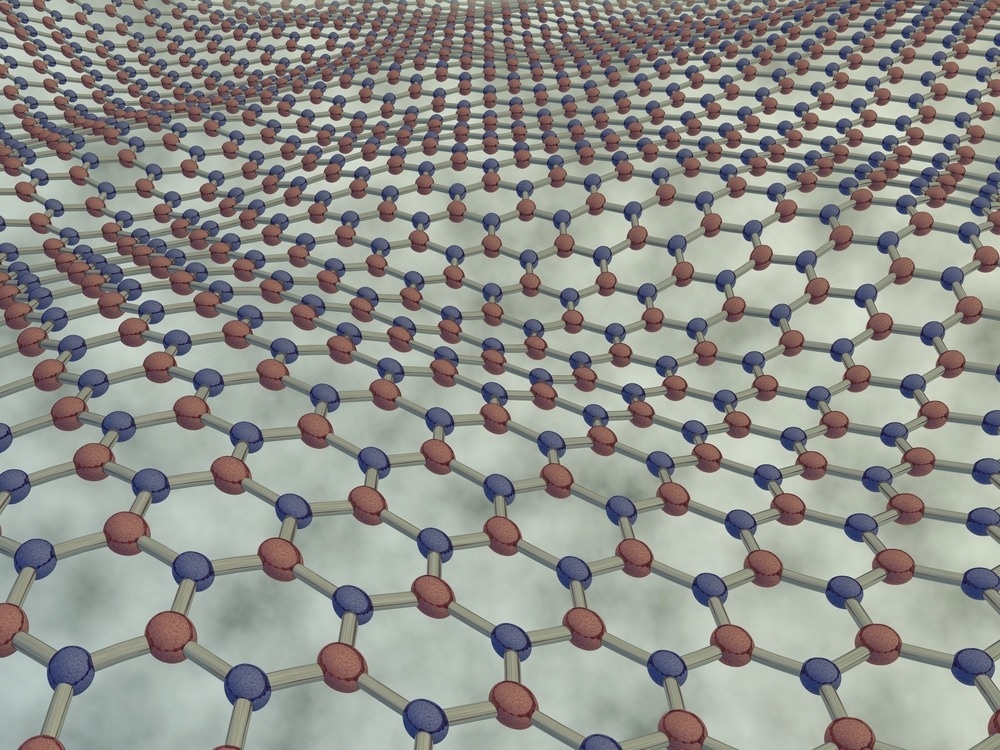
Image Credit: ogwen/Shutterstock.com
What is White Graphene?
Hexagonal Boron Nitride (hBN) is a layered material with a structure analogous to that of graphene. Within each layer, it is composed of alternating boron and nitrogen atoms that are arranged in a sp2 bonded network. The bond length between boron and nitrogen is 1.44 A°, whereas the bond length between carbon atoms in graphene is 1.42 A°.
Within each layer, the atoms of boron and nitrogen are held together by strong covalent bonds, while the layers themselves are held together by relatively weak van der Waals forces.
Graphene is a semiconductor with a zero-band gap, whereas hBN is an insulator with a large band gap of 5.97 eV, indicating its potential as high-quality dielectric material.
The hBN and graphene lattice mismatch is only 1.7 percent. Interestingly, hBN opens the bandgap in graphene when it is used as a substrate.
Properties and Advantages of hBN
2D hBN shows nearly no optical absorption in the visible spectrum, allowing for high transparency, but it has absorption spectroscopy in the ultraviolet region.
The thermal conductivity of hBN at room temperature can reach 751 W/mK, making it a promising filler for thermal management materials and heat dissipation in electronics devices.
The elastic modulus of the 2D hBN was evaluated to be 0.8 TPa, with high strength of about 100 GPa, which is comparable to graphene experimental values. Because of its exceptional mechanical characteristics, 2D hBN has been employed to reinforce polymer films.
The 2D hBN is stable in the air up to 1000 °C and does not react with most chemicals, making it one of the thinnest coatings ever demonstrated to endure harsh environments.
Aside from its oxidation resistance, monolayer hBN can also be used as an ideal coating to increase the electrical resistance and friction of substrates. 2D hBN is a potential coating material because of its high chemical, thermal stability and outstanding coating characteristics.
Heterostructure of 2D hBN
The most appealing application of 2D hBN is the construction of van der Waals heterostructures. Recent advances have been made in integrating 2D hBN with other 2D materials, like 2D TMDCs and graphene, to create hybrid 2D materials. For example, the graphene/hBN heterostructure enables the creation of high-performance graphene-based electronic devices and is very likely to be used to fabricate atomically thin integrated circuits.
2D hBN materials are always negatively charged and can be used as carrier acceptors in a heterojunction to improve the separation of charge carriers in photocatalysis.
In addition, hBN layers are also an excellent gate dielectric and encapsulant for hetero-bilayers in van der Waals 2D materials.
State of the Art: Synthesis of hBN
Top-down and bottom-up synthesis strategies are the most common types of 2D hBN synthesis strategies. The "bottom-up" process is correlated with the self-assembly of hBN via chemical vapor deposition (CVD) through the decomposition of B3N3H6 on transition metals. For example, Ulsan National Institute of Science and Technology researchers recently reported the synthesis of a large area 2 cm × 5 cm single crystal monolayer hBN on Ni (111).
The "top-down" process typically breaks the interlayer interaction between adjacent hBN layers via external forces, resulting in hBN exfoliation. Micromechanical exfoliation, liquid-phase exfoliation, chemical exfoliation, ball-milling and other methods have traditionally been used in this process.
The "top-down" method is an efficient and simple method for preparing hBNNSs on a mass scale. In a recent study, for example, researchers from the Chinese Academy of Sciences proposed a scalable and controllable method for exfoliating high-quality hBNN from hBN flakes with an exfoliation yield of more than 58 percent and hBN sheets thickness of less than 10 nm.
Commercial Applications of hBN
Ceramic fillers for polymer thermal conductivity optimization are one of the most common applications of hBN.
hBN is also in high demand in the cosmetics industry. It is also used by nearly all major cosmetic product manufacturers, including make-up accessories and other skincare products.
To improve heat dissipation, hBN is widely used for electrical insulation in consumer electronics such as batteries and other high-performance components.
As an anti-corrosion coating, hBN reduces the need for regular oiling and other treatments by preventing rust corrosion in the gun barrel.
hBN sensors are utilized as methane (CH4) detectors due to their high sensitivity and high resistance change when exposed to methane.
Global Manufacturer of hBN
Grolltex is a leading producer of high-quality hexagonal boron nitride sheets, producing monolayer hBN films on copper with sizes up to 150 mm × 150 mm. Furthermore, they offer monolayer hBN films on Si/SiO2 wafers with diameters of 100, 150, and 200 mm. Grolltex also offer custom-sized hBN films on wafers up to 200 mm in size.
Other major manufacturers of hBN powder include Saint-Gobain S.A. (France), 3M (U.S.), Denka Company ltd. (Japan), Showa Denko K.K. (Japan), Momentive Performance Materials Inc. (U.S.), HC Starck GmbH (Germany), and Henze Boron Nitride Products AG (Germany).
Future Prospect
Due to its excellent thermal, electrical and mechanical properties, 2D hBN is regarded as an ideal contender for a wide range of applications. The widespread application of 2D hBN, however, is dependent on progress in mass scale synthesis of 2D hBN with controlled layer number. It is expected that continued progress in synthesizing high-quality hBN layers will soon enable the realization of graphene/hBN heterojunction-based electronic devices.
References and Further Reading
An, L., et al. (2022). Water-icing-triggered scalable and controllable exfoliation of hexagonal boron nitride nanosheets. Cell Reports Physical Science, p. 100941. https://doi.org/10.1016/j.xcrp.2022.100941
Ma, K. Y., et al. (2022). Epitaxial single-crystal hexagonal boron nitride multilayers on Ni (111). Nature, 606(7912), pp. 88-93. https://doi.org/10.1038/s41586-022-04745-7
Wang, H., et al. (2017). Recent progress in synthesis of two-dimensional hexagonal boron nitride. Journal of Semiconductors, 38(3), p. 031003.
Ren, J., et al. (2021). 2D Boron nitride heterostructures: Recent advances and future challenges. Small Structures, 2(11), p. 2100068. https://doi.org/10.1002/sstr.202100068
Roy, S., et al. (2021). Structure, Properties and Applications of Two‐Dimensional Hexagonal Boron Nitride. Advanced Materials, 33(44), p. 2101589. https://doi.org/10.1002/adma.202101589
Disclaimer: The views expressed here are those of the author expressed in their private capacity and do not necessarily represent the views of AZoM.com Limited T/A AZoNetwork the owner and operator of this website. This disclaimer forms part of the Terms and conditions of use of this website.