Cutting-edge tools like FTIR spectroscopy and digital twin simulations are helping engineers fine-tune thin-film deposition, unlocking greater precision and efficiency in semiconductor manufacturing at the nanoscale.
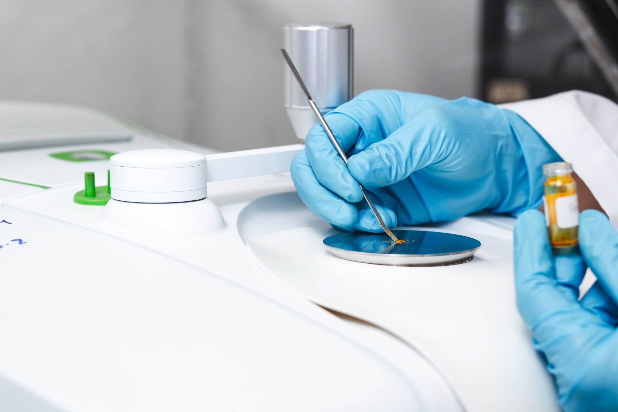
Image Credit: S. Singha/Shutterstock.com
In-Situ FTIR: Monitoring ALD and CVD at the Molecular Level
As chips shrink to the nanometer scale, precise control over every fabrication step becomes essential.
Atomic layer deposition (ALD) has emerged as a cornerstone of nanoelectronics, enabling the production of highly efficient semiconductors and critical components for integrated circuits (ICs). Its applications range from gate dielectrics in transistors to spacers for multi-patterning ICs.1
In-situ FTIR spectroscopy is central to understanding and improving ALD. Because ALD relies on complex surface chemistry, FTIR offers molecular-level insight into reaction dynamics.
For instance, one study on boron-doped Al2O3 films revealed a weak FTIR peak at 1498 cm-1 and a distinctive B–O stretching mode at 1348 cm-1. This demonstrated the precursor decomposition during deposition, concurrently revealing the surface functionalization during its growth.2
FTIR Analysis in Novel ALD Thin-Film Deposition Processes
Researchers are also applying FTIR to newer ALD techniques, such as plasma-enhanced ALD (PE-ALD) for carbon films.
In a recent experiment, α’-dichloro-p-xylene (DCX) was deposited on a SiO2 surface and modified using N2/H2 plasma. FTIR monitoring captured a drop in the Si–OH bond signal at 3740 cm-1 and a saturation of CH bending at 1250 cm-1. These signals evidence that DCX formed a monolayer via dehydrochlorination with hydroxyl groups.3
This demonstrates FTIR’s ability to track real-time chemical changes in advanced ALD processes, making it a powerful diagnostic tool in semiconductor manufacturing.
Effectiveness of FTIR for CVD Thin Film Deposition
FTIR has been key in analyzing CVD processes for thin-film deposition in semiconductor manufacturing. The spectroscopic technique underpins the production of silicon-based thin films and light emitters essential for optoelectronics.
One study used FTIR to examine doped silicon carbide films grown on silicon wafers. It provided detailed information on precursor consumption rates and bonding configurations, including Si–C and Si–N, and confirmed stable photoluminescence across the spectrum. The data captured ensured that the produced films met the exacting standards of modern semiconductor devices.4
Digital Twin Technology for Modern Thin Film Deposition and Semiconductor Manufacturing
Digital twin technology, essentially a live, virtual replica of a physical system, has become another key player in high-yield, low-defect semiconductor production.5
It uses sensors to integrate real-world processes and varying parameters with virtual process control and mechanism technology. This allows the user to analyze past and present process parameters and predict technological behaviour in complicated, real-world processes.
In thin-film deposition, digital twins provide precise, real-time control over important variables like substrate temperature and deposition rate, helping to maintain uniformity, optimize efficiency, and consistently produce high-quality films on the nanoscale.6
Classical FTIR Spectroscopy-based Monitoring and Control Loop Systems
The rapid growth in the semiconductor manufacturing market has led to a boost in the development of thin-film production. Despite widespread use of ALD, CVD, and PE-ALD, few studies have explored how feedback control loops can enhance these processes.
In the early 2000s, FTIR spectroscopy was used for in situ monitoring and control of semiconductor fabrication and thin-film deposition. FTIR instrumentation integrated with automated spectral analysis software was successfully demonstrated as a sensing solution for monitoring thin-film properties such as thickness, composition, and temperature.7
In the study, experts implemented a run-to-run closed-loop control system for a single-wafer epitaxial silicon process, integrating infrared-based thickness and doping profiling metrology setups.
This enabled closed-loop control in epitaxial silicon processes, where FTIR-based systems not only guided semiconductor manufacturing and thin-film development process control but also monitored exhaust gases for byproduct detection and fault classification.7
Download your PDF copy now!
CFD-Based Closed Loop Feedback for Thin Film Deposition
More recent efforts have combined multiscale computational fluid dynamics (CFD) simulations with run-to-run (R2R) and proportional-integral (PI) controllers. In experiments with hafnium oxide films, scientists used a multiscale CFD model to adjust precursor and carrier gas ratios in real time, ensuring optimal thickness and uniformity batch after batch.
The multiscale CFD model confirmed that the integrated PI and R2R control system effectively rejected process disturbances and maintained conformity during the thin-film deposition process during semiconductor manufacturing.
Compared to conventional sensor-based systems, this combined feedback loop achieved roughly 60 % faster response times, demonstrating the potential of integrated CFD-based control to maintain process stability and efficiency.8
This indicates that the spectral feedback loop is essential in controlling combustion and steam conditions and flow rate to optimize thin-film composition, while the precursor flow rate optimization leads to precise control over the thin-film thickness.
SIEMENS' AI-Powered Digital Twin
Siemens has introduced a novel digital twin technology to define and optimize production systems, such as semiconductor manufacturing and automotive assembly lines.
It efficiently reduces the need for prototype testing by providing a virtual environment incorporating mechanical, electrical, and electronic software and manufacturing to optimize processes like thin-film deposition.
By integrating AI and data analytics platforms, the tool can analyze and feed back performance data from real products through the control loop, implementing a continuous loop for improvement and optimization.
The AI analytics platform, taking key information from historical and contemporary data, can reduce maintenance downtime, predict upcoming maintenance, and devise predictive maintenance schedules to optimize production.
It could also be used to analyze feed rates, precursor flow rates, and temperature conditions to optimize resource consumption and ensure the quality of the final thin-film product. It may be key for companies to reach their required sustainable development goals.9
The combined use of FTIR spectroscopy and digital twin technology is reshaping how thin films are designed and fabricated at the nanoscale. Together, they allow for finer control over film composition and uniformity, faster production cycles, and fewer interruptions.
Further Reading
- Li, J. et. al. (2023). Atomic layer deposition of thin films: from a chemistry perspective. International Journal of Extreme Manufacturing, 5(3). 032003. Available at: https://iopscience.iop.org/article/10.1088/2631-7990/acd88e
- Li, X. et. al. (2023). Atomic Layer Deposition of Boron-Doped Al2O3 Dielectric Films. Advanced Materials Interfaces, 10(18), 2300173. Available at: https://doi.org/10.1002/admi.202300173
- Hu, L., Tsutsumi, T., Kobayashi, N., Ishikawa, K., & Hori, M. (2025). Plasma-enhanced atomic layer deposition of carbon films employing a cyclic process of N2/H2 plasma and α, α’-dichloro-p-xylene as a precursor. Applied Surface Science, 681, 161485. Available at: https://doi.org/10.1016/j.apsusc.2024.161485
- Kar, A. et. al. (2024). Synthesis of silicon carbide thin film as a source for white light emission. Optical Materials, 155, 115795. Available at: https://doi.org/10.1016/j.optmat.2024.115795
- Ansys. (2025). What is a Semiconductor Digital Twin? [Online]. Available at: https://www.ansys.com/simulation-topics/what-is-a-semiconductor-digital-twin [Accessed on: June 08, 2025].
- Kumar, H. et. al. (2025). SiC Thin Films: Nanosecond Pulsed Laser-Deposition via Digital Twin Approach and Atom Probe Tomography Characterizations. Thin Solid Films, 140620. Available at: https://doi.org/10.1016/j.tsf.2025.140620
- Rosenthal, P. et. al. (1998). Infrared spectroscopy for process control and fault detection of advanced semiconductor processes. In AIP Conference Proceedings. 449(1). 213-219. American Institute of Physics. Available at: https://doi.org/10.1063/1.56898
- Yun, S. et. al. (2021). Integration of feedback control and run-to-run control for plasma enhanced atomic layer deposition of hafnium oxide thin films. Computers & Chemical Engineering. 148. 107267. Available at: https://doi.org/10.1016/j.compchemeng.2021.107267
- Siemens, White Paper (2024). Supercharging the Industry Transformation with the Comprehensive Digital Twin. [Online]. Available at: https://assets.new.siemens.com/siemens/assets/api/uuid:cda2b14c-23bf-4685-8fdf-adb7fd25e3a7/Whitepaper-Digital-Twin-EN.pdf [Accessed on: June 11, 2025].
Disclaimer: The views expressed here are those of the author expressed in their private capacity and do not necessarily represent the views of AZoM.com Limited T/A AZoNetwork the owner and operator of this website. This disclaimer forms part of the Terms and conditions of use of this website.