Mar 3 2009
Just as x-ray technology, MRI and sonography transformed the practice of medicine, a newly created approach for seeing the invisible promises great potential for finding new ways to improve the health of human and microelectronic patients alike. Semiconductor Research Corporation (SRC), the world's leading university-research consortium for semiconductors and related technologies, today joined with Northwestern University to announce successful demonstration of a unique ultrasound holography approach that enables scientists to view the tiniest of buried structures.
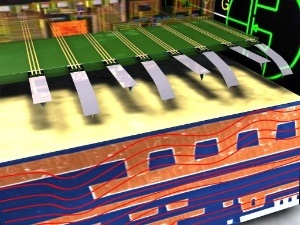 New sub-surface, embedded defect analysis will be more accurate than any other imaging process, spurring a spin-off company to commercialize the technology. (Photo: Business Wire)
The resulting three-dimensional information will provide benefits ranging from greater yields for semiconductor manufacturers to more effective treatments for medical patients.
Using a novel, non-destructive approach that combines, for the first time ever, scanning-probe microscopy (SPM) with ultrasound and holography, researchers at Northwestern University have demonstrated the ability to view subsurface particles as small as 15-20 nanometers (a nanometer is one billionth of a meter). Such capabilities have not previously been possible without slicing the sample, which changes both the composition and structure and sacrifices characteristics of the studied subject.
What makes the new approach revolutionary is the combined use of the SPM, ultrasound and holography. SPM offers nanoscale resolution. Ultrasound is non-destructive, transparent to all materials and sensitive to embedded structures, including nano-sized defects. Holography also can provide sophisticated three-dimensional representations of the buried information. Together, the three technologies offer unprecedented visibility to the increasingly important tiny parts of nature.
As there’s neither a similar approach nor such a high class of result available anywhere, a high-tech start-up company has been launched to further the commercial applications for these methods. Named NanoSonix Inc., the spin-off will develop a nanoscale-imaging toolset capable of rapid evaluation of defects and flaws below the surfaces as well as valuable recognition of buried patterns and structures.
“Microelectronics, in particular, is a flaw-intolerant technology where even nanoscale defects can compromise the performance and yield of the devices,” said Dr. Dan Herr, director of nanomanufacturing sciences for SRC-GRC, an entity of SRC. “The ability to see such defects is critical for yield enhancement as devices become smaller and such metrology techniques and tools become even more crucial. These results are very good news for multiple industries.”
Utilizing the new technology, the microelectronics and nano-electro-mechanical systems (NEMS) industries can improve performance of their devices, time to yield and, ultimately, yield rates by deploying this technique in process development and as an in-line quality control tool. Thanks to the non-destructive imaging approach, the pharmaceutical industry should benefit from better understanding of how drugs distribute, accumulate and clear from different parts of the body.
“Biomedicine is moving towards use of nano-bio-structures to interrogate cells and deliver therapeutic cargo. This requires a non-invasive view inside the cells to monitor what’s happening under physiologically viable conditions,” said Dr. Vinayak Dravid, professor of materials science and engineering and the director of the NUANCE Center at Northwestern University. “With the new imaging technology, it’s possible to sharply increase our understanding of the bio-distribution of new drugs and the important interactions of nanoparticles and cells during intended or desirable therapeutic delivery or unintended environmental uptake.”
Next steps in development of the technology include system integration, material handling, faster scanning and high through-put of results. In-line tools and methods for addressing these needs will be created by NanoSonix. For instance, in the next 12 months, the spin-off will develop an add-on module for existing commercial SPM equipment in order to meet associated off-line metrology requirements. Availability of such an add-on module will make this technology accessible to a wider community, not only in semiconductor metrology but also in bio-application for both academia and industry to look deep below surfaces non-destructively with nanoscale resolution.