Aug 31 2010
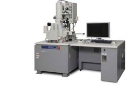
The new SU8040 Field Emission Scanning Electron Microscope (FE-SEM) from Hitachi High-Technologies features a newly developed Regulus (REGULated Ultra Stable) Specimen Stage for unprecedented smooth sample control even at ultra-high magnification. The SU8040 is an outstanding tool for the leading nanotechnology industries, such as the semiconductor industry and cutting-edge nanotechnology material analysis.
Nanotechnology and semiconductor samples contain structures of nanometre dimensions which need to be imaged and measured at hundreds of thousand times magnification and ultra high resolution. The Regulus stage provides the extremely fine specimen stage control that is needed for smooth operation at such high magnifications in order to be able to locate and maintain the regions of interest. The Regulus stage uses a proven conventional motor drive with a newly developed motor drivetrain to give seamless stage operation throughout the magnification range.
Also new for the SU8040 is the optional ‘cell count assist’ software. This software recognises the repeat patterns of DRAM/SRAM samples, and makes use of the outstanding Regulus stage performance to allow automated identification of patterns for measurement and defect analysis. The automated approach eliminates tedious manual searching for the regions of interest.
The SU8040 offers outstanding imaging capabilities, with a resolution capability of 1.3nm at a landing voltage of 1.0kV. The SU8040 benefits from Hitachi’s revolutionary in-lens triple detection system, originally introduced on the SU8000. This novel, ultra-sensitive detection system allows high efficiency simultaneous multi-signal imaging and energy filtering. The extraordinary versatility of this detection system not only provides high sensitivity detection for ultra-low current imaging of sensitive materials, but also allows the imaging of structures and surface properties never seen before – taking SEM imaging into whole new areas of materials examination and development.
Secondary electrons, low angle and high angle backscattered electrons can be detected and displayed either independently or as a mixed signal image using a primary beam of as little as 100v, providing the capability to observe the absolute surface structure as well as properties such as surface potential contrast.