Imec along with its collaborators in the GaN industrial affiliation program (IIAP) has processed some power devices on 200mm GaN-on-Si wafers. Using these wafers, standard CMOS tools were used to process operational GaN MISHEMTs (metal-insulator-semiconductor HEMT).
The used methods comply with the stringent contamination regulations in a typical CMOS processing line. These power devices on 200mm CMOS-compatible wafers are a significant landmark, supporting low-cost development of power devices on high-output 200mm fabs.
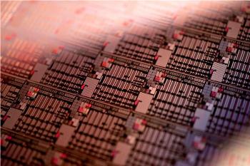 Imec processes first power devices on 200mm CMOS-compatible GaN-on-Si
GaN holds high promise for future power devices and its functionality is better than silicon. Recently, Imec has developed 200mm GaN-on-Si wafers without any fissures on its surface and a bow measuring around 50µm. The wafers were developed by means of an innovative MOCVD system created by Applied Materials. Ability to utilize 200mm wafers facilitates processing of high-output 200mm fabs, resulting in significant reduction in cost in contrast to processing tiny wafers in exclusive processing lines.
Another requirement for low-cost processing is that power devices can be developed with methods that comply with typical CMOS methods and tools. IMOS substantiated this prerequisite by processing its newly developed GaN-on-Si wafers by means of typical CMOS tools, generating operational GaN MISHEMTs. All devices were assessed for its ability to process wafers and only minor modifications in software and hardware are needed. Traditionally, gold is utilized for developing gate structures and ohmic contacts in power systems. But processing of GaN is not compatible with traditional CMOS processing method. In order to avoid this, the company formed the ohmic contact on a metallization system free of Au and altered the Schottky gate to a metal-insulator-semiconductor (MIS) structure. The gate dielectric based MIS structure does not include gold and the launch of the MISHEMT structure minimizes the high leakage current of traditional HEMTs.