Researchers of K.U.Leuven, while examining the nanomaterials’ optical properties, have discovered that surface plasmons leave behind imprints on the nanostructures’ surface. This discovery has led to the development of a high resolution microscope that is suited for imaging the nanostructures’ electric fields.
 Surface plasmon patterns can be imprinted on metallic nanostructures for subsequent high resolution imaging with standard surface probe techniques
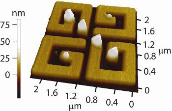
Nanomaterials, comprising thin layers or minute particles, are likely to acquire unexpected characteristics. In recent years, optical nanomaterials have become a sought-after topic because of their applications and counterintuitive optical behavior. They are based on surface plasmon resonances, a characteristic by which light can excite surface electron waves collectively in metallic nanostructures. The electron waves can be manipulated at the nanoscale because they possess shorter wavelengths than light but identical frequency. By using plasmons, light can be stored, modified, and captured in nanostructures. This technology is suitable for an array of applications such as cancer treatment.
Imaging the surface plasmons offers a direct method to study and map the electric fields. However, imaging the surface plasmons in high resolution is both complex and expensive. But now, a user-friendly and effective procedure for imaging plasmonic patterns has been established by Ventsislav K. Valev and his colleagues.
The scientists have found that by lighting nanostructures, which are manufactured using palladium or nickel, the surface plasmon pattern gets imprinted by itself on the nanostructure. The imprinting takes place by movement of the material from the nanostructure to the areas where considerable plasmon improvements have been done. Imaging of the decorated plasmons is conducted using conventional surface probe methodologies such as atomic force microscopy or scanning electron microscopy.