New Technique to Visualize Individual Layers and Buried Interfaces of Graphene Devices
Scientists from the University of Manchester have shown that it is possible to use ‘wonder material’ graphene as a building block to build novel three-dimensional crystal structures.
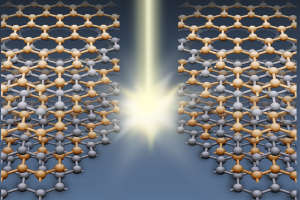
The new technique enables fabrication of electrical devices with novel properties by placing sheets of graphene between insulating layers, thus providing new approach to physics research.
In a paper reported in Nature Materials, the researchers have described a new side-view imaging method that is capable of visualizing the individual graphene atomic layers of the nanomaterial-based devices. What they discovered was the structures were near-perfect even when over 10 variety of layers were utilized to fabricate the stack.
This finding signifies that the latest methods of separating graphene are an important progress towards atomic level engineering. This advancement provides more credence to graphene’s potential as key component in advanced computer chips. The side-view imaging technique involves the removal of a thin section from the center of the device. The researchers extracted the desired section of the device by cutting the graphene surface and plowing a trench on either side of the section using an ion beam.
Dr Sarah Haigh from the School of Materials of The University of Manchester stated that since the slices are of mere 100-atom thick, the researchers were able to image the individual graphene atomic layers in projection. The researchers discovered that the observed roughness of the nanomaterial has a correlation with its conductivity. They also found that the layers were completely clean and any trash available from production separated as isolated pockets, thus maintaining device performance. The researchers intend to utilize this novel side-view imaging technique to optimize the performance of their graphene devices.
Written by
Will has a B.Sc. in Chemistry from the University of Durham, and a M.Sc. in Green Chemistry from the University of York. Naturally, Will is our resident Chemistry expert but, a love of science and the internet makes Will the all-rounder of the team. In his spare time Will likes to play the drums, cook and brew cider.
Please use one of the following formats to cite this article in your essay, paper or report:
APA
Soutter, Will. (2019, February 12). New Technique to Visualize Individual Layers and Buried Interfaces of Graphene Devices. AZoNano. Retrieved on June 22, 2026 from https://www.azonano.com/news.aspx?newsID=25322.
MLA
Soutter, Will. "New Technique to Visualize Individual Layers and Buried Interfaces of Graphene Devices". AZoNano. 22 June 2026. <https://www.azonano.com/news.aspx?newsID=25322>.
Chicago
Soutter, Will. "New Technique to Visualize Individual Layers and Buried Interfaces of Graphene Devices". AZoNano. https://www.azonano.com/news.aspx?newsID=25322. (accessed June 22, 2026).
Harvard
Soutter, Will. 2019. New Technique to Visualize Individual Layers and Buried Interfaces of Graphene Devices. AZoNano, viewed 22 June 2026, https://www.azonano.com/news.aspx?newsID=25322.
We're committed to providing free access to quality science. By registering and providing insight into
your preferences you're joining a community of over 1m science interested individuals and help us to
provide you with insightful content whilst keeping our service free.
or
Terms
While we only use edited and approved content for Azthena
answers, it may on occasions provide incorrect responses.
Please confirm any data provided with the related suppliers or
authors. We do not provide medical advice, if you search for
medical information you must always consult a medical
professional before acting on any information provided.
Your questions, but not your email details will be shared with
OpenAI and retained for 30 days in accordance with their
privacy principles.
Please do not ask questions that use sensitive or confidential
information.
Read the full Terms & Conditions.