The National Physical Laboratory (NPL) has collaborated with Chalmers University of Technology and Linköping University in Sweden to help develop a fast and inexpensive tool for quality control of graphene grown on silicon carbide.
 The design of a device overlaid on an optical image of a graphene sample - bilayer patches are clearly visible on monolayer background (image courtesy of Arseniy Lartsev, Chalmers University of Technology)
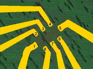
Graphene was originally made using a method called 'exfoliation' which involves pulling graphite apart, for example with sticky tape, until you are left with a carbon layer one atom thick. While this produces high quality graphene, the method is not suitable for mass production and commercial applications.
An alternative method is to grow graphene epitaxially (in layers) from a crystal of silicon carbide at high temperature. NPL and collaborators recently used graphene grown this way to develop a superior quantum Hall resistance standard. However, to ramp up the production of graphene to the levels and perfection required by the electronics industry, fast and inexpensive measurement tools for quality control are required.
The new quality control technique, published in Nano Letters, is based on optical microscopy and can be used to understand the effect of the silicon carbide substrate on the quality of the graphene layer. It was previously thought that the contrast of graphene on silicon carbide was too low to be observed directly with an optical microscope. But, by analysing optical images and comparing them to electrical measurements, the technique was able to identify single graphene layers only 0.3 nanometres thick.
In a practical demonstration, the researchers built graphene devices on specific parts of the silicon carbide, which they located using the optical microscopy technique. As well as identifying single layers of graphene, they were able to visualise features such as stepped terraces on the silicon carbide substrate and areas of multilayer graphene. They then tested the electrical characteristics of the devices built on each area. The results confirmed the ability of the optical microscope to detect areas of different topography and layer coverage of the graphene.
This research demonstrates how optical microscopy can detect defects during the growth of graphene on silicon carbide. The results produced are comparable to other more developed techniques but are quicker to obtain and non-invasive. This makes the optical microscopy technique a prime candidate for industrial quality control.
NPL's contribution to the project was to quantify the optical images and to validate the optical microscopy data using well-established techniques such as scanning Kelvin probe microscopy. This work was supported by EU Seventh Framework Programme (FP7) project ConceptGraphene and the IRD graphene project of the UK National Measurement Office.
NPL recently joined the Graphene Stakeholders Association to promote the responsible development of graphene and graphene-enabled technologies.