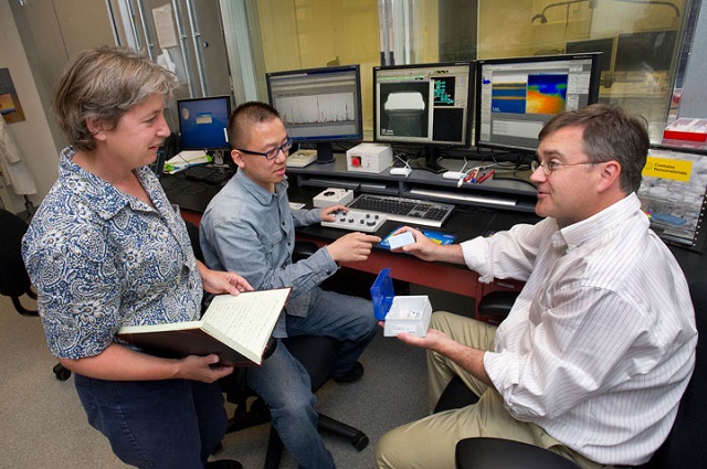
 IBM scientist Frances Ross (left) with Brookhaven Lab scientists Dong Su (center) and Eric Stach in the Center for Functional Nanomaterials.
Researchers have developed an innovative technique that makes it possible to self-organize and customize complicated structures at the nanoscale. This breakthrough was facilitated through an international collaboration headed by IBM and the University of Cambridge. The study paves the way to customize material properties and functionalities for a variety of semiconductor device applications.
The latest method helps in growing different combinations of materials in needle-shaped crystals known as nanowires. Nanowires are tiny structures measuring just a few billionths of a metre in diameter. It is possible to grow semiconductors into nanowires, which result in building blocks for energy harvesting, optical, and electrical devices. The research team has identified a way to grow tiny crystals inside the nanowire, producing a crystal rod-like structure having an integrated series of gems. Results of the study have been published in the journal Nature Materials.
The key to building functional nanoscale devices is to control materials and their interfaces at the atomic level. We've developed a method of engineering inclusions of different materials so that we can make complex structures in a very precise way.
Dr. Stephan Hofmann of the Department of Engineering
Vapour-liquid-solid (VLS) synthesis is a process used for growing nanowires. In this process, a small catalytic droplet is utilized to both seed and feed the nanowire, allowing it to self-assemble, a single atomic layer at a time. The VLS process enables excellent control across the resulting nanowire. Properties like diameter, composition, crystal structure, growth direction, kinking and branching can be controlled by adjusting the self-assembly conditions. Nanowires that are better controlled allow for new potential applications.
The method developed by Hofmann and his colleagues from IBM and Cambridge can be regarded as an expansion of the theory underlying traditional VLS growth. The small catalytic droplet used by the researchers helps in growing the nanowire and at the same time aids in forming novel materials within the nanowire. As the nanowire is grown further, these small crystals that form in the liquid subsequently adhere to the nanowire and get integrated. This docking process mediated by the catalyst can self-optimize to produce highly perfect interfaces for the integrated crystals.
In order to resolve the difficulties of this process, two customized electron microscopes were used by the researchers: one at Brookhaven National Laboratory and the other at IBM's TJ Watson Research Center. With the help of these instruments, the team was able to record ultra-speed movies of the nanowire growth as it takes place atom-by-atom. The research group discovered that when the catalyst is used as a mixing bowl, with the amount and order of individual ingredient programmed into a preferred recipe, it resulted in complicated structures containing nanowires with integrated quantum dots or nanoscale crystals of controlled position and size.
The technique allows two different materials to be incorporated into the same nanowire, even if the lattice structures of the two crystals don't perfectly match. It's a flexible platform that can be used for different technologies.
Hofmann
Potential uses of this method range from single-electron transistors and atomically perfect integrated interconnects through to semiconductor lasers, high-density memories, tunnel diodes, light emission, having the capability to develop 3D device structures.
This process has enabled us to understand the behaviour of nanoscale materials in unprecedented detail, and that knowledge can now be applied to other processes.
Hofmann.