Nov 20 2017
In the immediate future, a main origin of reliability issues in carbon nanotube (CNT)-based VLSI interconnects may be noise and crosstalk. Maintenance of signal integrity in integrated circuits (ICs) has been difficult due to the reduction of the size of components in IC to nanometer scale, in addition to high-density integration.
The probability of crosstalk between adjacent wires is very high. Consequently, the crosstalk leads to increase in the peak noise in the transient signals passing through the interconnects. During multiple crosstalk occurrences, the noise is transferred through a number of stages of wires and the complication is exacerbated into logic failure.
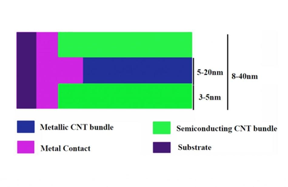 CNT bundle surrounded by semiconducting CNTs. CREDIT: Dr. Uma Sathyakam P., Dr. Partha S. Mallick, Bentham Science Publishers.
However, this can be overcome by placing semiconducting CNTs around an interconnect, thereby considerably reducing crosstalk. To date, semiconducting CNTs have been used for making futuristic field effect transistors. Semiconducting CNTs are non-conducting and have medium to large band gaps as well as a small dielectric constant. This enables them to function as insulating shields to electric fields.
Due to the fact that the semiconducting CNTs are one-dimensional nanowires, they have extremely high anisotropic characteristics not only along their axis but also along their radius. The dielectric polarizability—or the number of polarizable bonds in a material—is observed to be extremely small along the radius of the CNTs as against their axis. Therefore, semiconducting CNTs are polarizable along their radius to a lesser degree, thereby indicating that their dielectric constants are small. The well-known Clausius-Mossotti relation can be adopted to calculate the dielectric constant by using the dielectric polarizability. Moreover, the relation also shows that a CNT’s dielectric constant is directly proportional to the measure of its radius. Therefore, semiconducting CNTs that have a small diameter are evidently optimal for use as the low-k dielectric medium in between two CNT interconnects.
The contact geometry is altered such that the density of the metal atoms is greater at the centre where metallic CNTs exist. The contact includes fewer metal atoms at the boundary where semiconducting CNTs exist. This arrangement assists in forming a Schottky barrier at the contact semiconducting CNTs interface, thereby preventing any carrier movement.
Ultimately, experimental outcomes indicate that the radial dielectric constant can be extremely low—that is, 2.82—if (2,2) CNTs are adopted as shields. The coupling capacitance between adjacent wires is governed not only by the thickness of the interconnect but also by the thickness of the semiconducting CNTs shield. The use of semiconducting CNTs can decrease the crosstalk between CNTs wires by nearly 28%. In addition, the peak noise generated due to the crosstalk was observed to be lesser by 25% for semiconducting CNTs shielded interconnects at varied input voltages of 0.8, 0.5, and 0.3 V.