Nanodevices produced using BCP thin films have found several applications in the electronic industry because of their superior qualities such as small unit size, low operating energy, and better functionality.
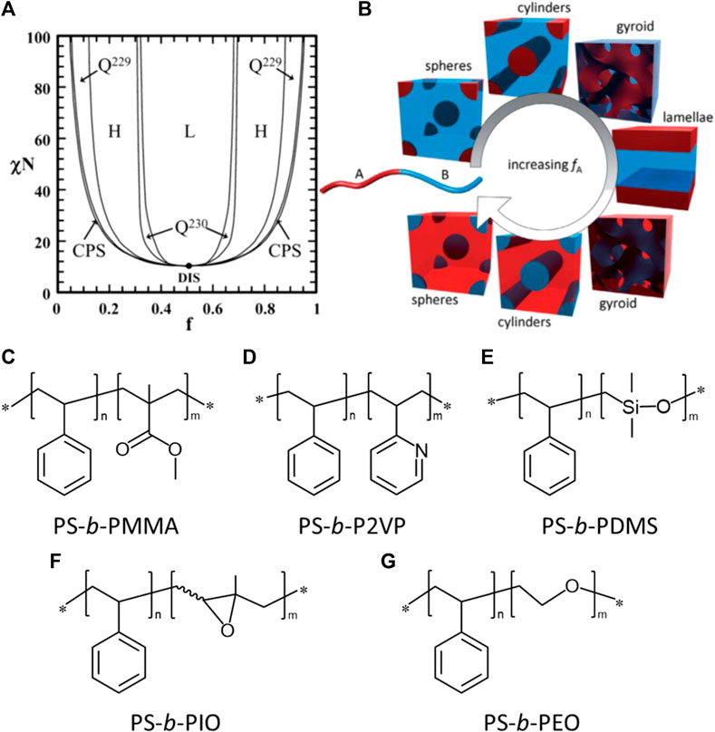
(A) Phase diagram of PS-b-PMMA system, indicating regions of interaction parameter (χ) and volume fraction (f) that give rise to formation of different morphologies where L: lamellae, H: hexagonally packed cylinders, Q230: double gyroid phase, Q229: body-centered spheres, CPS: closed-packed spheres, and DIS: disordered phase (B) represents evolution of different morphologies as volume fraction of component A is increased. (Reproduced from ref. 1) (C–G) chemical structures of various commonly used block copolymers that are addressed throughout this manuscript. Image Credit: Ashwanth, S. et al.
Material Templating using BCP Thin Films
Due to the potential of self-assembled block copolymer (BCP) thin films to instantaneously produce different nanostructures, they have appeared as a novel templating method with several benefits. This includes a decrease in supply and operating expenses, a small size that is not achieved by standard methods, and simple integration into the present technology for mass production.
However, BCP-based nanodevices are not readily suitable for many applications due to their restricted structural qualities.
In comparison to its synthetic alternatives, polystyrene BCP thin film has weak mechanical, thermodynamic, and electrical performance.
Postassembly treatment is usually necessary to convert these polymeric structures into more usable synthetic nanoparticles.
BCP Derived Methods for Nanodevice Fabrication
In recent years, there has been a surge in the production of nanodevices employing block copolymer-derived technology. A basic BCP film is composed of two insoluble polymer blocks that are chemically bonded and are stacked on top of each other. Using a heat processing process or by exposing the thin films to liquid-vapor, BCP thin films can be self-assembled on a variety of substrates, including silicon wafers.
It is possible to fabricate nanowire-based electronics such as semiconductors and monitors using BCP thin films because of their wire-like structure at the nanoscale. The spherical shape nanomaterials are employed for designing high-density nanodot arrays for application in storage devices, such as flash memory.
However, in order to use BCP-based nanoparticles for practical electronic applications, it is important to change their geometries for them to display conductive, semi-conductive, and optical characteristics.
Modification Strategies for BCP-based nanostructures
One of the easiest ways to convert BCP patterns into electroactive nanostructures is achieved with the lift-off technique.
The lift-off technique involves depositing a thin layer of necessary material onto a substrate having plastic patterns and then washing away the portion of the prepared film that remains on the material when the polymer is disintegrated in a solvent.
A material bonding approach directed by the disintegration, dispersion, and reactivity of metal precursors with polymeric substrates called infiltration, is another means to turn BCP patterns into synthetic nanomaterials.
Based on the kind of precursors utilized, the infiltration procedure may be divided into two types: vapor-phase infiltration (VPI) and liquid-phase infiltration (LPI).
These methods allow inorganic materials to grow inside an organic matrix, resulting in organic-inorganic composites. Due to the merging of various initial elements at the cellular scale, such composites often have remarkable material characteristics.
VPI has been shown to improve a variety of polymeric characteristics, including physical, toxicological, structural, optical, and thermodynamic properties. Advanced sensors, photodiodes, gas screens, and gas filters are some of the uses for VPI hybrids. Furthermore, the BCP self-assembly method may be used in conjunction with the VPI method to make intricate, 3D synthetic nanomaterials that are beneficial in electrical device applications.
In the liquid-phase infiltration (LPI) technique, inorganic salt solutions are obtained by adding the salts to water or other solvents.
Direct contact between inorganic materials in the form of liquid metal salts and reactive functional molecules allows for penetration. Combining precision processing of BCP thin films with LPI provides perpendicularly aligned nanorods and nanoparticles with consistent material characteristics, which are useful in various applications.
Conclusion and Future Perspective
Self-assembly modification methods such as thin-film accumulation, VPI, and LPI hybridization, and plasma engraving pattern technique have facilitated the production of semiconductor materials, metal alloys, and conductive thermoplastic nanodevices for use in devices such as photonic detectors and solar cells, amongst other applications.
Because of their sizable adaptability, simplicity of manufacturing, and variety of synthetic pattern generation and conversion techniques, self-assembled BCP thin films have the potential to be used in a broad range of electric, mechanical, and photonic products in the future.
Continue reading: Dielectric Film Measurement: What is it and Why is it Important?
Reference
Ashwanth, S. et al. (2021). Templating Functional Materials Using Self-Assembled Block Copolymer Thin-Film for Nanodevices. Frontiers in Nanotechnology, 3, 94. Available at: https://www.frontiersin.org/articles/10.3389/fnano.2021.766690/full
Disclaimer: The views expressed here are those of the author expressed in their private capacity and do not necessarily represent the views of AZoM.com Limited T/A AZoNetwork the owner and operator of this website. This disclaimer forms part of the Terms and conditions of use of this website.