LMs have displayed significant potential for investigating fundamental physics and device applications. In LMs, such as transition metal dichalcogenides (TMDs) and hexagonal boron nitride (hBN), weaker vdW forces hold together the layers, while every layer is bounded by covalent in-plane bonds.
The properties of LMs can be tuned by controlling interlayer twist angle, which produces a spatially modulated interlayer registry, referred to as moiré superlattice. This leads to Mott-like insulator states and superconductivity in twisted graphene bilayers and interlayer excitonic long-lived states in monolayer heterostructures.
hBN, a wide-bandgap insulating LM with a unique set of electrical, mechanical, and optical properties, is used extensively as an encapsulation material in graphene and related materials. hBN has also gained prominence in the context of moiré physics. For instance, scattering near-field optical microscopy (s-SNOM) revealed the in-plane optical phonon frequency variation for different stacking in a twisted-hBN (t-hBN) moiré superlattice.
Similarly, Kelvin probe force microscopy (KPFM) and electrostatic force microscopy (EFM) were also performed on t-hBN to address the existence of two permanent opposite out-of-plane polarization arising from the moiré pattern. However, the effect of moiré superlattices on the local vdW interactions in twisted LMs such as t-hBNs was not explored until now.

© Chiodini, S., Kerfoot, J., Venturi, G. et al. (2022)
Novel Method to Investigate the Moiré Modulation of vdW Potential of LMs
In this study, researchers investigated the moiré interlayer modulation of the t-hBN vdW potential using tapping mode atomic force microscopy (AFM) phase imaging, a tool used extensively for nanoscale force characterization, to directly visualize and quantify the vdW interlayer interactions.
A t-hBN sample composed of eight nanometers bottom hBN layer and two nanometers top hBN layer was used for the study. AFM images were obtained in tapping mode at a scan rate of 0.5−1 hertz.
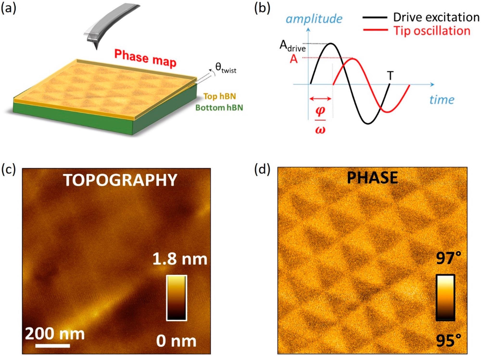
The modulation was observed on the vdW potential at the surface of the top t-hBN sample. The energy dissipation associated with the vdW potential modulation was quantified after calibrating the AFM parameters. Researchers quantified the dissipated energy and visualized the modulated vdW potential resulting from the t-hBN moiré superlattices at the air-top hBN layer interface by tuning the phase channel to the local vdW dissipation.
In tapping mode AFM, the phase channel sine represents the energy dissipated in the sample-tip interaction, which depends on the sample-tip distance specific to the force probed. Thus, the tapping mode AFM allows long-range/noncontact vdW forces to be differentiated from the local interactions such as viscoelasticity and capillary forces. A physical interpretation of the vdW dissipation contrast nanoscale origin was obtained based on the sample-tip interaction analysis.

Tapping mode AFM imaging of t-hBN. (a) Schematic of t-hBN (2 nm/8 nm, θtwist ∼ 0°) sample. (b) Plot of the two main signals involved in AFM phase-imaging, i.e., drive excitation (black) and tip oscillation response (red). Adrive and A are reported, together φ, T = 2π/ω, ω = 2πν (v is the cantilever first resonance frequency). (c) Representative AFM topography of top hBN, showing a flat morphology. (d) Corresponding AFM (attractive) phase channel where the moiré superlattice is visible. Imaging parameters for (c,d): A0 = 5.3 nm, A = 5.1 nm, free phase ∼86°. Cantilever: Scanasyst fluid (Bruker, k ∼ 0.7 N·m–1). © Chiodini, S., Kerfoot, J., Venturi, G. et al. (2022)
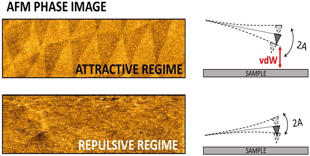
The sample-tip interaction analysis demonstrated that the Debye force between the permanent interlayer electric dipoles and the neutral tip was the main source of the imaging contrast. The phase images and topography of the air/hBN interface over a 1 micrometer × 1 micrometer scanned area in repulsive regime (RR) and attractive regime (AR) were obtained.
After the acquisition of phase images, the dissipation maps were reconstructed. AFM force-spectroscopy was performed to distinguish the vdW forces and capillary forces as dissipative mechanisms. KPFM/phase/AFM measurements were taken at 25 degrees Celsius and calibration procedures were performed at the end of experiments to avoid any damage to the tips. The imaging technique was used to observe the moire ́ domains in other LMs such as twisted-tungsten diselenide (t-WSe2) to evaluate the general applicability of the technique.
Significance of the Study
The moiré superlattice of t-hBN and t-WSe2 induced the spatial modulation of the vdW potential without tip or sample biasing. The repulsive interactions were eliminated by tuning the sample-tip force to AR to primarily probe the long-range vdW forces, which allowed the visualization of two distinct triangular vdW domains BA and AB that emerged from the moiré superlattice. The BA regions were the more dissipative compared to AB.
Although the topography did not provide any contrast associated with the moiré superlattice in both AR and RR, the phase images demonstrated a pattern of triangular domains only in the AR. The topography remained unchanged and the moiré contrast disappeared completely in the phase map when the oscillation regime shifted from AR to RR. The moiré pattern was recovered when the AR imaging parameters were restored. In the dissipation maps, the triangular domains of the moiré superlattice were observed only in the AR.
The origin of the moiré pattern contrast in the phase map was primarily attributed to the interlayer vdW potential in the moiré superlattice. The vdW forces emerged from the quantum mechanical interaction between transient or permanent electric dipoles between molecules. The vdW dissipation regime extension was limited to the first five to ten nanometers above the top hBN layer surface.
A ferroelectric dipole layer was present at the interface of the top and bottom hBN layer owing to the marginal twist angle between two crystal structures, which indicated that moiré phase-image contrast emerged from the Debye dissipative vdW interaction between the sample and the tip.
Moreover, the twisting also led to electrostatic field nanopatterning at the sample/environment interface. The modulation generates a local field nanopatterning with the tunability and periodicity of the moiré pattern. By twisting the hBN layers, the size, domain extension, and the electrostatic potential modulation on the samples can be engineered, which provides a tool for surface functionalization by locally tuning the electrostatic interaction on a large scale with the environment while maintaining nanometer resolution.
To summarize, the findings of this study demonstrated that vdW potential modulation through layer twisting at the interface with the environment could create scalable electrostatic domains, which could be used for surface functionalization and local adhesion engineering by affecting the nanoparticle or molecule deposition.
Reference
Chiodini, S., Kerfoot, J., Venturi, G. et al. (2022) Moiré Modulation of Van Der Waals Potential in Twisted Hexagonal Boron Nitride. ACS Nano https://pubs.acs.org/doi/10.1021/acsnano.1c11107
Disclaimer: The views expressed here are those of the author expressed in their private capacity and do not necessarily represent the views of AZoM.com Limited T/A AZoNetwork the owner and operator of this website. This disclaimer forms part of the Terms and conditions of use of this website.