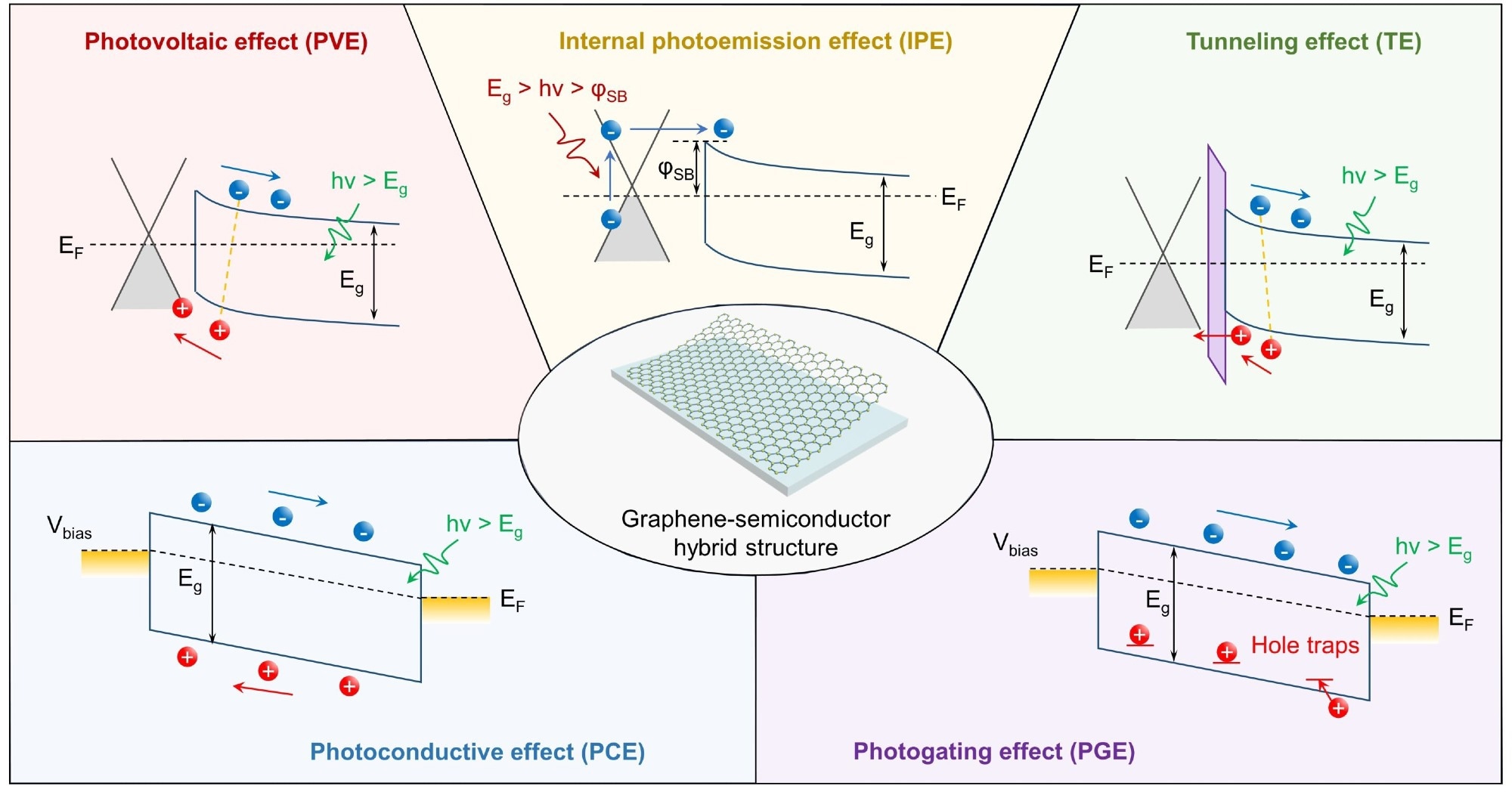
The recent study published in Advanced Devices & Instrumentation summarizes a decade of advancements in graphene-semiconductor hybrid photodetectors. It begins by outlining the key performance metrics for photodetectors to lay the groundwork for an accurate evaluation. The review then elucidates the photoelectric conversion mechanism specific to graphene-semiconductor hybrid photodetectors.
 As a representative two-dimensional material, graphene possesses unique optical and electrical properties that hold immense promise in various fields, particularly in photodetection. Nonetheless, its atomic-level thickness results in weak light absorption, seriously limiting the enhancement of key performance indicators for graphene photodetectors. Image Credit: Advanced Devices & Instrumentation
After that, it explores the fundamental ideas behind these detectors’ different configurations, providing information on typical devices. The study concludes by outlining potential avenues for future graphene-semiconductor hybrid photodetectors’ development.
Graphene-semiconductor hybrid photodetectors provide several benefits.
- Graphene enhances other semiconductor materials, fostering new phenomena in photocurrent generation, transport, and collection and leading to the creation of innovative devices.
- Graphene's ability to integrate easily with other semiconductors—without the need for precise lattice matching—offers considerable flexibility in choosing semiconductor materials.
- The compatibility of graphene with silicon-based complementary metal-oxide-semiconductor (CMOS) processes, along with the established process technology of traditional semiconductors, provides a solid foundation for transitioning graphene-semiconductor hybrid photodetectors from lab to practical applications.
These innovations have propelled significant advancements in broadband detection, achieving GHz-level working bandwidth, ultra-high responsivity, and gain bandwidth production. Despite these achievements, challenges remain in developing devices that combine high performance, multifunctionality, and wafer-level manufacturing.
Addressing these challenges through the development of new techniques and processes is crucial for optimizing performance and enhancing functionality, setting the stage for future breakthroughs in photodetection technology.
Journal Reference:
Fu, J., et. al. (2024) Photodetectors Based on Graphene–Semiconductor Hybrid Structures: Recent Progress and Future Outlook. Advanced Devices & Instrumentation. doi:10.34133/adi.0031