Turning nanodisks into nanostars, researchers have designed a tunable platform for sharper, more reliable chemical sensing.
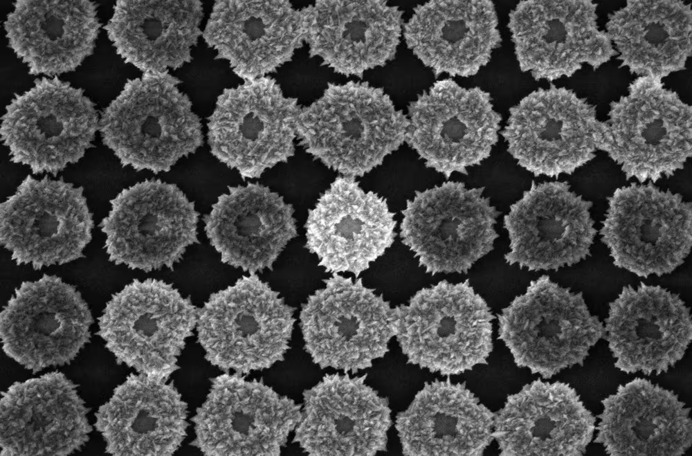 High-resolution SEM images capturing how gold nanodisks transform into more complex nanoscale architectures. Image Credit: Alexandre Chícharo/Diéguez group at NIL
Researchers at INL, part of the Diéguez group and led by Sara Abalde-Cela, have engineered a plasmonic substrate that substantially enhances the stability and reproducibility of SERS-based sensing.
The study, published in Advanced Optical Materials, describes a fabrication method integrating precise nanopatterning with regulated chemical growth.
Surface-enhanced Raman scattering (SERS) spectroscopy is a potent technique for highly sensitive and swift chemical analysis.
Its efficacy stems from the interaction of light with minute metallic structures, which generates electromagnetic fields that significantly amplify the Raman signal.
However, translating this principle into dependable and scalable sensing platforms has been a persistent obstacle in SERS, hindering its broader application in areas such as medical diagnostics, environmental monitoring, and molecular biosensing.
The fabrication process commences with electron beam lithography to produce highly ordered nanodisk arrays. Subsequently, these disks are converted into nanostars, characterized by sharp tips that can generate exceptionally intense electromagnetic fields, thereby creating "hot spots."
Compared to nanodisks, which produce weaker and more homogeneous field enhancements, the nanostars show highly localized electromagnetic intensification at their tips.
Both simulations, run by Temple Douglas from Nieder group, and experimental SERS measurements confirmed this transformation and validated its impact on signal amplification.
Sara Abalde-Cela, Group Lead, International Iberian Nanotechnology Laboratory
The method questions the idea that top-down fabrication is excessively expensive or unfeasible for broader applications. Using optimized exposure settings and a dots-on-the-fly technique, the researchers decreased fabrication duration and expense, preserving nanoscale accuracy.
This strategy enables precise control over particle spacing, shape, and distribution – parameters crucial for generating robust and reliable SERS signals. The nanostar arrays illustrate how meticulously designed geometry can directly yield enhanced sensing capability.
The investigation elucidates a distinct route to application-specific and expandable SERS infrastructures.
The INL scientists emphasize prospective avenues like incorporating surface modification and merging the process with extensive lithographic procedures. For example, nanoimprint or deep-UV lithography can be used to further enhance production efficiency.
The group combines accurate nanofabrication and controlled chemistry, laying the groundwork for dependable, high-performance SERS substrates and enabling novel molecular detection methods in biomedical diagnostics, chemical analysis, and optical sensing.
Journal Reference:
Chícharo, A., et al. (2025). Precision-Engineered Plasmonic Nanostar Arrays for High-Performance SERS Sensing. Advanced Optical Materials. DOI:10.1002/adom.202501275.