Jul 15 2008
IMEC, in collaboration with JSR Corporation, realized a simplified process using only one etch step to reduce the cost of double patterning. 32nm lines and spaces were printed with a double exposure/single etch process, effectively freezing the resist after the first exposure. This simplified process paves the way for an industrial take-up of double patterning for the 32nm technology node.
 (left) 32nm node 2D logic cells after litho-freezing-litho-etch. The lines from the two layers are perfectly merged on the stitching points. (right) The same cell patterned with litho-etch-litho-etch. The oxide hard mask has not been removed to show the lines obtained with the first litho step.
Double patterning will be the primary lithography candidate for the 32nm technology node. But when using two litho and two etch steps, this technique will be expensive and slow. Therefore, IMEC is developing alternative process flows that reduce the cost-of-ownership by eliminating the intermediate etch step and replacing it with a process step in the litho track.
One way to eliminate the extra etch step is through freezing the resist after the first exposure. With this technique, IMEC has demonstrated 32nm node logic patterning. The freezing material used to reach this result has been developed by JSR Corporation. It prevents the resist from expanding (i.e. CD growth) or shrinking. And when the second resist layer is added, the two do not interact. Also, the freezing material is compatible with the lithography hardware.
The step of freezing the resist is done in the litho track. After exposing the first pattern, the resist is coated with the freezing material. Next, the wafer is baked to freeze the resist. Then the excess freezing material is removed using a developer. In the following step, a second resist layer is added and the second exposure is done. To prevent the second resist layer solvent from washing away the first resist, the freezing material changes the properties of the first resist layer so that it becomes non-soluble in the second resist layer.
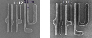
This technique allowed printing 32nm dense lines using dipole illumination at 1.0NA. CDU for the 44nm HP lines was excellent (3s = 2.4nm). Moreover, 32nm node 2D logic cells as well as 32nm dense lines could be etched into poly. Lines resulting from the first and second lithography step cannot be distinguished, illustrating the good resolution obtained with this technique.
IMEC is currently transferring this process to its newly installed 1.35 NA immersion scanner (ASML XT:1900i) to explore this solution for sub-32nm half pitches (towards 22nm node).