Dec 4 2008
SUSS MicroTec Test Systems (FWB:SMH)(GER:SMH) has revealed the ProberBench(TM) Operating Environment, a full-featured software suite for efficient, intuitive and safe wafer-level probing. In 1995, SUSS revolutionized wafer-level test by introducing the first Windows-based prober control software. Now, more than a decade later, SUSS has developed the latest software revolution for engineering wafer probe systems for the 21st century.
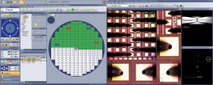 The new ProberBench(TM) Operating Environment from SUSS MicroTec, a full-featured software suite for efficient, intuitive and safe wafer-level probing (Photo: Business Wire)
“The ProberBench™ Operating Environment is a complete redesign of our software interface and architecture,” said Dr. Stojan Kanev, Director of Marketing and Product Management at SUSS MicroTec Test Systems. “Development was based primarily on an intensive, three-month user study in the laboratories of several large and small semiconductor design houses and manufacturers.”
The results of the study showed that users were unhappy with the current solutions in the market due to feature overload and confusing interfaces. Many companies were experiencing high rates of probe card and wafer damage that was linked directly to the users’ misinterpretation of signals and software feedback. In addition, every interviewee expressed the desire for automation of procedures so that the probe system could run unattended over nights and weekends, which would lead to significant productivity gains.
The ProberBench™ Operating Environment addresses all of these needs by empowering the operator to work more effectively and safely when setting up and executing wafer-level test routines. The new software includes the Control Center, placing all navigation and control elements at the user’s fingertips and providing instant feedback about wafer and probe positions for worry-free, safe wafer navigation and probing. Also included is the new SPECTRUM™ Vision System, which is the main vision application and supports up to four live video feeds like ContactView™ – a horizontal view of the probe tips and wafer for eliminating expensive probe card and wafer damage – and an upward-looking camera for viewing the tips of fine-pitch, vertical probe cards.
Furthermore, the ProberBench™ Operating Environment has several optional automation tools such a tool for automatically aligning the wafer and generating a wafer map. It is also designed to communicate with test executive software like Agilent’s IC-CAP, Keithley’s KITE, ProPlus’ BSIMPro and many others. Combining this feature with SUSS MicroTec’s unique Automated Thermal Management™ and ReAlign™ Technology enables unattended test routines over multiple temperatures that can be run overnight and on weekends, significantly increasing system utilization and ultimately improving time to market and return on investment.
A beta version of the ProberBench™ Operating Environment will be shown at SEMICON Japan from 3-5 December. First shipments of the software are expected in the first quarter of 2009.