DOI :
10.2240/azojono0123
Nov 14 2007
The conductive and field emission properties of individual single and multi-walled carbon nanotubes, grown by chemical vapor and supercritical fluid deposition techniques, have been assessed using an in-situ transmission electron microscope-scanning tunneling microscope (TEM-STM) technique. The conductivity and field emission measurements were obtained from nanotube-electrode distance and contact observations. Experimental field emission characteristics for all carbon nanotubes investigated fitted well to the Fowler-Nordheim equation when different work functions were applied. Differences in field emission and conductive properties are analyzed and related to the structure of the carbon nanotubes. The method presented here is suitable for in situ selection of CNT with desired properties for particular electronic applications.
Background
Carbon nanotubes (CNTs) are attractive materials with a wide range of potential applications. CNT based various electronic devices, such as transistors [1-5], logical circuits [6] nanoelectromechanical devices, [7-9] sensors [10,11] has been demonstrated. In 1995 field emission from CNTs was reported [12,13] and nanotubes becomes promising candidates as a field electron emitters. [14-17]. The high aspect ratio (length to diameter) of the CNTs results in a high field enhancement factor, beneficial to field emission.
These applications demand an unusual combination of material properties, such as structural rigidity, electric conductivity and small density, possessed only by CNTs. Electronic devices should also withstand high temperatures caused by Joule heating and high tensile stresses to avoid device failure.
Since nanotubes can be grown by different methods with various structures, the selection of an appropriate type of CNT for a selective application is a challenging task. The CNTs can be prepared by various methods such as arc discharge, laser ablation, chemical vapor deposition (CVD), supercritical fluid (SCF) and others [18-20] with CVD the most widely used method of production.
For a large number of applications, such as field emission, investigations have been mostly performed on CNT films or arrays. Direct comparison measurements on individual nanotubes are more informative than average characterisation on arrays or large quantities of CNTs.
Field emission and conductive properties as well as degradation and failure parameters of individual nanotubes have been investigated by a number of groups (see, for example, [21-24]. However, to the best of our knowledge, there has yet to be a study carried out on different nanotubes investigated under identical experimental conditions. Separate facts are currently available on the lifetime, degradation and failure of individual nanotube emitters [21,23,24] as well as on the conductive properties, electrical breakdown mechanism and parameters of individual nanotubes during two-point characterization [22], but it is often problematic to compare properties of different nanotubes due to experimental conditions not being the same.
In this paper we report a systematic study of the conductive and field emission properties for single-walled, multi-walled, including bamboo-structured carbon nanotubes (BCNTs) and single-walled CNT filled with C60 molecules. All structures were investigated under identical conditions and compared. Recently developed in situ techniques [25-29] in which the contact place and shape can be adjusted and observed during measurements was used in our experiments. The nanotubes were prepared by chemical vapour deposition (CVD) and supercritical fluid (SCF) methods.
A scanning tunneling microscope, built in a sample holder of a transmission electron microscope (TEM-STM) [29,30], was used to manipulate and probe the nanotubes as illustrated in figure 1. The nanotubes were bonded onto a gold tip using electrically conductive adhesive CW2400, through which the electrical contact was made; the second tip was used as the counter electrode and could be directly observed in TEM.
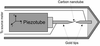 Figure 1. Schematics of the measurement set-up inside Transmission Electron Microscope.
Experiments were carried out in a Philips TEM-301 microscope operating at 80 kV, equipped with a Keen View II CCD camera for image acquisition. Vacuum in the sample chamber was approximately 10-3 Pa. The bias voltage and sample current were controlled by a source meter (Keithley 6430).
The carbon nanotubes were produced by the CVD and SCF technique. The lengths of the nanotubes were between 600 nm and 8 µm, and the radiuses were between 7 and 50 nm. Non purified multi-walled carbon nanotubes from Aldrich were measured for reference.
CVD grown wall and multiwall CNTs were synthesized on MgO supported Co/Mo (tube type nanotubes) CNTs and Pd/Mo (bamboo type nanotubes) catalysts. MgO was prepared by the decomposition of Mg2(OH)2CO3 at 450 ºC for 6 hr [31].
SWCNTs Nanotubes
An aqueous solutions of Co(NO3)2.6H20 and (NH4)Mo6O24.H2O were prepared and mixed with the MgO support with a Co:Mo molar ratio of 3:2 followed by drying in an oven at 80oC. The dried precursor powder was then calcined at 550 ºC. 0.3g of the catalyst was placed in a quartz tube and heated to 800 ºC in a reducing atmosphere of H2/Ar at a flow rate of 300 ml min-1 for 30 min. Methane was then fed into the tube at a flow rate of 50 ml min-1. The growth period for SWNT formation was set at 60 min, after which the furnace was cooled to room temperature. To gain pure SWNT material, the as-prepared material was treated with 6 M HNO3 and was washed by water to remove the catalyst.
Tube Type MWCNTs
An aqueous solutions of Co(NO3)2.6H20 and (NH4)Mo6O24.H2O were prepared and mixed with the MgO support with a Co:Mo weight ratio of 3:4 followed by drying in an oven at 80oC. The dried precursor powder was then calcined at 550 ºC. 0.3g of the catalyst was placed in a quartz tube and heated to 800 ºC in a reducing atmosphere of H2/Ar at a flow rate of 300 ml min-1 for 30 min. Methane was then fed into the tube at a flow rate of 200 ml min-1 with a H2/Ar flow rate of 100 ml min-1. The growth period for MWNT formation was set at 60 min, after which the furnace was cooled to room temperature. To gain pure MWNT material, the as-prepared material was treated with 6 M HNO3 and was washed by water to remove the catalyst.
Bamboo Type MWCNT
An aqueous solution of Pd(NO3)2.xH2O and (NH4)Mo6O24.H2O was mixed with the MgO support, followed by sonication for 30 min and drying. The dried precursor powder was sintered at 500 ºC for 6 hr. 0.3g of the catalyst was placed in a quartz tube and heated to 900 ºC in a reducing atmosphere of H2/Ar at a flow rate of 300 ml min-1 for 30 min. Methane was then fed into the tube at a flow rate of 100 ml min-1. The growth period for BCNTs formation was set at 30 min, after which the furnace was cooled to room temperature. To gain pure BCNTs material, the as-prepared material was treated with 6 M HNO3 and was washed by water to remove the catalyst.
SCF Grown Nanotubes
SCF grown nanotubes were prepared on a MgO supported 3 wt.% Co and 4 wt.% Mo catalyst [20]. In a typical SCF deposition experiment, 0.5 g Co/MgO catalyst was placed into a high pressure reactor (Inconel 625 GR2- Snap-tite, Inc.), and was reduced using H2/Ar (V/V=20/180 ml min-1) at 750 °C for 30 min. CO as the carbon source was first added to a 450 ml stainless steel reservoir at 40 °C in a temperature controlled water bath. A flow through system was established by connecting the inlet and outlet valves of the carbon source reservoir, which included a piston, to a 260-ml ISCO syringe pump (Lincoln, NE) and the reaction vessel respectively. A back pressure regulator maintained the system at constant pressure and controlled the flow rate of CO through the system. The reaction time was set to 60 min. After the reactor was cooled down to room temperature, the carbon/catalyst powder was treated with 6M HNO3.
Results and Discussion
Field Emission Properties
For field emission experiments a high electric potential (up to 250 V) was applied between the CNT and the counter electrode. The TEM-SPM setup allows accurate control and measurement of the position of the CNT relative to the anode and other surrounding objects (fig 2a). The local field was estimated using  [21], where
  is the applied potential,
  is the interelectrode distance,
  is the field enhancement factor. The geometrical field enhancement factor γ for nanotubes was determined by their length L and radius r as γ = (0.87L/r + 4.5) [32,33]. In our case, the field enhancement factor exceeds 100 for most of nanotubes investigated except for CVD grown tube like MWNTs for which γ=20 (table 1).
Figure 2b and table 1 show comparison of field emission currents as a function of local field for all investigated types of carbon nanotubes.
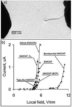 Figure 2. a) TEM image of a CVD grown multiwall carbon nanotube during field emission measurements; b) current dependence on local field for different types of CNT. Solid lines are fitting with Fowler-Nordheim theory calculated using work function 8.1 eV for bamboo like nanotubes and for others - 5.1 eV.
Typically, the field emission for MWCNT grown on Co/Mo catalyst sets in at local fields of 1.5 - 4.1 V/nm (table 1) and saturates at local fields of 3.0 – 4.6 V/nm, which is comparable to the literature data for multi-walled carbon nanotubes [21]. Our data for CVD grown SWNTs not filled and filled with C60 molecules shows that field emission starts at almost identical voltages to those observed for MWNTs. Commercial CVD grown nanotubes (from Aldrich) and MWCNTs grown by the novel supercritical fluid (SCF) deposition method exhibit almost identical field emission characteristics to those grown by the CVD method on a Co/Mo catalyst (fig. 2b). Field emission and conductive characteristics of CNTs is affected by the degree of graphitization [34].
According to our findings, the situation is more complicated. Raman spectrum for CVD grown SWCNTs and SCF grown nanotubes (Figure 3) shows difference in G and D band height ratios. G and D bands correspond to sp2 (conductive structures) and sp3 (nonconductive structures) bonding in CNTs. Though G/D band ratio and the consequent higher degree of graphitization is observed for CNTs grown on Co/Mo catalyst, we do not observe remarkable diffrences in field emission properties of CVD and SCF grown nanotubes. G/D ratio for bamboo like structures is even higher than for CVD grown SWCNTs, however, field emission for bamboo shaped MWCNTs grown on MgO supported Pd/Mo catalyst by the CVD method sets up at much higher local fields 7-8 V/nm (figure 2b).
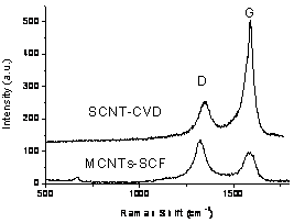 Figure 3. Raman spectra of CVD-grown single wall CNTs prepared by methane decomposition at 800 C, and SCF-grown multiwall CNTs by CO disproportion at 750 C.
The dependence of current on local field obtained for all investigated nanotubes fitted well to the Fowler-Nordheim model (see, Figure 2b solid lines), which states that the current (I) per emitter varies with the local field at the emitter’s surface area (A) [36,37]:
 (1)
(1)
where Φ is the work function, V is the applied voltage; and d is the interelectrode distance.
For all nanotubes, except the BCNTs, field emission characteristics fit to the Fowler-Nordheim model when a value for the work function of graphite 5.1 eV [5] was used. The peculiar local field needed for emission from the BCNTs required a work function value of 8.1 eV to be used. The junctions in these BCNTs are likely to influence the effective L/r ratio, which determines the field enhancement factor, making the emission threshold fields larger.
The average field emission currents were determined at saturation (see table 1) and varied from 10 nA to 500 nA for CVD grown tube like MWCNTs, from 100 nA to 1.5 µA for BCNTs, and from 150 nA to 2 µA for SCF grown MWCNTs. Commercially available (Aldrich) MWCNTs exhibit higher field emission currents - up to 10 μA. Previously reported values for field emission saturation currents for CVD grown nanotubes varied in a very large interval from 2 nA to 9 µA [19]. Field emission saturation currents for CVD grown SWCNTs varied from 100 nA to 5 µA for empty and up to 10 µA for C60 filled SWCNTs. During field emission characterization of individual nanotubes field emission currents at saturation were fluctuating in time for approximately 50% of average values, similar to those reported previously [38].
Table 1. Field emission characteristics of CNTs grown at different conditions.
|
|
|
Emission start up local field, V/nm
|
1.5-4.1
|
3.0-4.9
|
3.5- .4
|
4.5-5.5
|
2.5-4.5
|
8–10
|
|
Field emission current, μA
|
0.01-0.5
|
0.1 - 5.0
|
0.1 - 10.0
|
5 - 15
|
0.15 - 2.0
|
0.1 – 1.5
|
|
Breaking current, μA
|
0.1-1.0
|
0.15-10.0
|
2.5-10.0
|
10-0 25
|
0.45-3.5
|
0.45-2.0
|
|
Breaking local field, V/nm
|
3.0 – 6.0
|
4.0 - 6.0
|
4.0 - 9.0
|
6.0 - 8.0
|
3.5 - 8.0
|
9.0 - 12.0
|
|
Breaking place
|
in contact
|
in contact
|
gradual destruction
|
gradual destruction
|
in contact
|
in contact, gradual destruction
|
|
Field enhancement factor
|
20±5
|
110±30
|
90±10
|
105±15
|
135±30
|
150±30
|
At high local fields failure of the nanotubes was observed (Fig 4, table 1). Failure currents were approximately 2 times higher than saturation currents. Failure local fields are presented in table 1 and varied from 3-4.6 V/nm for tube-like MWCNTs and up to 12 V/nm for bamboo-like MWCNTs. Literature values of breaking local fields for CVD grown nanotubes from different groups varied in the interval of 3 to 10 V/nm [19,21].
Breaking local fields for SWCNTs were comparable with MWCNTs (up to 6 V/nm), while C60-filled SWNTs exhibited a higher stability with breaking local fields up to 9 V/nm. A gradual degradation of C60-filled SWNTS and BCNTs emitters at high applied voltages (200-250V) were observed as shown in figure 4 (see also table 1.) while all other nanotubes failed at the weak contact between the CNT and the gold tip; in this case the CNT fully removes from the gold tip when the emission current is not very high.
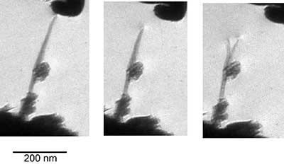 Figure 4. A gradual destruction of a single-walled CNT filled with C60 molecules bundle at constant voltage (200 V) applied. The time between images is 10 s.
Electrical Characterization Using a Two Probe Method
In order to measure the electric conductivity of the individual CNTs, the nanotube was brought into direct contact with a counter electrode as shown in figure 5a. I(V) characteristics of all types of CNTs addressed in this paper are shown in Figure 5c.
Table 2. Conductive and breaking characteristics of CVD-grown CNTs.
|
|
|
Breaking voltage, V
|
4.5 - 6.0
|
5.0 - 11.0
|
4.0 - 4.5
|
≥25
|
0.7 - 8.0
|
0.7 - 5.0
|
|
Breaking current, μA
|
12 - 19
|
7 - 80
|
10 - 18
|
≥0.3
|
0.0003- 0.01
|
0.0005 - 0.005
|
|
Breaking place
|
near the contact
|
near the middle
|
near the middle
|
near the middle
|
near the middle
|
near the middle, near the contact
|
Accordingly resistances for all nanotubes can be divided into two groups. The resistance of the first group (tube-like MWCNTs and SWCNTs) of nanotubes varied in the interval of 250 kΩ – 1MΩ, which is typical for two-probe characterization of CVD grown CNTs [19]. The resistance in this group decreases in the order of CVD grown tube like MWCNTs, empty and filled with C60 SWCNTs (Figure 5c).
C60-filled SWNTS exhibited lower resistance in comparison to unfilled SWNTS. For CVD grown BCNTs, commercial MWCNTs and SCF grown MWNTs, the resistance measured was higher by 3 orders of magnitude in comparison to data for first group of nanotubes reported above. Reason for such differences for SCF and commercial nanotubes may be a lower degree of graphitization in comparison to nanotubes grown on C0/Mo catalyst.
As shown in Raman spectrums (Figure 3), SCF nanotubes exhibit lower degree of graphitization in comparison to nanotubes grown on Co/Mo catalyst by the CVD method. Our opinion is that the commercial and SCF grown nanotubes have fragmentary outer shells with a high density of defects. In case of a two-point characterization, the counter electrode contacts direct to defective outer shells instead of current-carrying less defective inner shells.
To provide electron transport through inner shells, a higher voltage is required. As reported previously, outer layers of carbon nanotubes are dominant in electron transport and therefore determine the conductivity of the nanotubes [22]. Possibly inner layers are participating in field emission therefore significant differences in field emission between CVD and SCF grown nanotubes was not observed (Figure 2b) in comparison to the difference in resistances (Figure 5c). It is possible that the junctions present in bamboo like structures evenly decrease the conductivity in the outer and inner walls of the CNTs. This property may increase the resistance of field emission and conductivity.
Nanotube Quality
To characterize the quality of the nanotubes, failure currents and voltages were determined (see table 2). Nanotube failure currents were up to 20 µA for CVD-grown SWNTs and MWNTs and up to 80 µA for C60-filled SWNTs. Failure voltages were up to 5 V for SWNTs and up to 10 V for C60-filled SWNTs (see table 2). Bamboo type CNTs are stable even at 25 V which means that these nanotubes can be used in high electric field applications. Figure 5b shows that the nanotube is disrupted near its middle, which has been observed for all types of nanotubes. This result suggests that the tubes were resistively heated and that the temperature becomes locally high enough to vaporize the graphite wall; consequently, the location of damage by Joule heating is not determined by the presence of defects in the CNT. Consequently, the location of the defects does not have an effect on the breaking point of the CNT under observation. In other works [19,21] nanotube failures were found near the middle and in the contact regions.
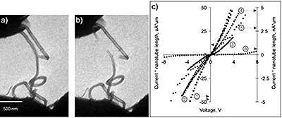 Figure 5. a) MWCNT grown by CVD method and b) nanotube breaking during two-probe measurements; c) comparison between I(V) curves of different types of CNTs: 1 - singlewall CNTs filled with C60 molecules, 2 - empty singlewall CNTs, 3 - multiwall CNTs grown on Co/Mo catalyst, 4 - Aldrich commercially available multiwall CNTs, 5 - multiwall CNTs grown on Pd/Mo catalyst, 6 - multiwall CNTs grown by supercritical fluid method.
Conclusions
The field emission and conductive properties of varieties of SWNTs and MWNTs were studied under identical conditions inside a transmission electron microscope. Conductivity and field emission properties were nanotube structure dependent. Differences in properties, whether conductive or field emission, depended on the structure of the outer layers, the presence of junctions in bamboo type nanotubes and whether the nanotubes had been filled with C60 molecules. Nanotubes filled with C60 molecules show improved conductive and field emission properties. Bamboo structures exhibited poorer field emission properties in comparison with the other CNT structures; however, these nanotubes were more stable at higher electrical fields. We suggest that the quality of the outer layers of nanotubes can decrease the conductivity of nanotubes by 3 orders of magnitude, without significantly affecting the field emission properties.
Filled single-walled and bamboo like multiwall carbon nanotubes exhibit higher breaking fields in comparison with empty single and tube like multiwall carbon nanotubes. During two-probe measurements the failure of nanotubes at high electric fields occurred at or near the nanotube middle. These results suggest that the breaking place is not determined by the location of defects inside the nanotubes but by Joule heating. Also, gradual destruction of nanotubes during field emission was observed for C60 filled SWNTs and bamboo type MWNTs. These experiments showed that TEM SPM equipped with DC electrodes has proven to be a valuable tool for systematic characterization of individual carbon nanotubes. It can be considered superior to lithography methods because of faster acquisition of results.
Acknowledgements
This work was supported by the EU Specific Targeted Research Project DESYGN-IT (No NMP4-CT-2004-505626) and Latvian National Program in Material Sciences. J.A. and J.P. Acknowledge support from ESF.
References
- Tans S. J., Verschueren A. R. M., Dekker C., “Room temperature transistor based on a single carbon nanotube”, Nature, 393, 49-52, 1998.
- Postma H. W. Ch., Teepen T., Yao Z., Grifoni M., Dekker C., “Carbon Nanotube Single-Electron Transistors at Room Temperature”, Science, 293, 76-79, 2001.
- Auvray S., Derycke V., Goffman M., Filoramo A., Jost O., and Bourgoin J.-P., “Chemical Optimization of Self-Assembled Carbon Nanotube Transistors”, Nano Lett., 5(3), 451-455, 2005.
- Xiao K., Liu Y., Hu P., Yu G., Fu L., and Zhu D., “High performance field-effect transistors made of a multiwall CNx/C nanotube intramolecular junction”, Appl. Phys. Lett., 83(23), 4824-4826, 2003.
- Weitz R. T., Zschieschang U., Effenberger F., Klauk H., Burghard M., Kern K., “High-Performance Carbon Nanotube Field Effect Transistors with a Thin Gate Dielectric Based on a Self-Assembled Monolayer’,Nano Lett., 7, 22-27, 2007.
- Bathold A., Hadley P., Nakanishi T., Dekker C., “Logic Circuits with Carbon Nanotube Transistors”, Science, 294, 1317-1320, 2001.
- Rueckes T., Kim K., Joslevich E., Tseng G. Y., Cheung C., and Lieber C. M., “Carbon Nanotube-Based Nonvolatile Random Access Memory for Molecular Computing”, Science, 289, 94, 2000.
- Lee S.W, Lee D.S., Morjan R.E., Jhang S.H., Sveningsson M., Nerushev O. A., Park Y.W., and Campbell E.E.B, “A Three Terminal Carbon Nanorelay”, Nano Lett. 4, 2027, 2004.
- Ke C., Espinosa H. D., “In Situ Electron Microscopy Electromechanical Characterization of a Bistable NEMS Device”, Small, 2(12), 1484 – 1489, 2006.
- Park M., Cola B., Siegmund T., Xu J., Maschmann M. R., Fisher T. S., and Kim H., “Effects of a Carbon Nanotube Layer on Electrical Contact Resistance Between Copper Substrates”, Nanotechnology, 17, 2294–2303, 2006.
- Brian H., Halsall H.B., Dong Z., Jazieh A., Tu Y., Wong D., Pixley S., Behbehani M.l, and Schulz M. J., “A Carbon Nanotube Needle Biosensor”, J. Nanosc. Nanotechn., 7, 2293–2300, 2007.
- Rinzler A.G., Hafner J.H.., Nikolaev P., Lou L., Kim S.G., Tomanek D., Nordlander P., Colbert D.T., Smalley R. E., “Unraveling Nanotubes – Field Emission from an Atomic Wire’, Science, 269(5230), 1550-1553, 1995.
- Deheer W.A., Chatelain A., Ugarte D., “A Carbon Nanotube Field Emission Electron Source”, Science, 270(5239), 1179-1180, 1995.
- Wong Y. M., Kang, W. P., Davidson J. L., Wisitsora-at A., Soh K. L., Fisher T. S., Li Q., Xu J. F., “Field Emitter Using Multiwalled Carbon Nanotubes Grown on the Silicon Tip Region by Microwave Plasma-Enhanced Chemical Vapor Deposition”, J. Vac. Sci. Technol. B, 21(1), 391-394, 2003.
- Bonard J. M., Weiss N. Kind H., Stockli T., Forro L., Kern K, Chatelain A., “Tuning the Field Emission Properties of Patterned Carbon Nantoube Films”, Adv. Mater., 13(3), 184-188., 2001.
- Wang Q. H., Corrigan T. D., Dai J. Y., Chang R. P. H., Krauss A. R., “Field Emission from Nanotube Bundle Emitters at Low Fields”, Appl. Phys. Lett., 70(24), 3308-3310, 1997.
- Pan Z. W. Au F. C. K., Lai H. L., Zhou, W. Y., Sun L. F., Liu, Z. Q., Tang D. S., Lee C. S., Lee S. T., Xie, S. S., “Amorphous Carbon Nanowires Investigated by Near-Edge-x-Ray-Absorption-Fine-Structures”, J. Phys. Chem. B, 105(8), 1519-1522, 2001.
- Iijima S., “Helical Microtubules of Graphitic Carbon”, Nature, 354(6348), 56-58, 1991.
- “Carbon Nanotubes”. Dresselhaus M.S., Dresselhaus G., Avouris Ph. Eds. Topics in Applied Physics, Springer Verlag, Berlin, 80, 1 – 430, 2001
- Li Z., Andzane J., Erts D., Tobin J.M. , Wang K., Morris M.A., Attard G., and Holmes J. D. „A New Supercritical Fluid Method for Growing Carbon Nanotubes”, Adv. Mater., in press.
- Bonard J. M., Klinke C., Dean K. A., and Coll B. F., “Degradation and Failure of Carbon Nanotube Field Emitters”, Phys. Rev. B, 67, 115406 – 1, 2003.
- Collins P.G., Arnold M.S., Avouris P., “Engineering Carbon Nanotubes and Nanotube Circuits Using Electrical Breakdown”, Science, 292 (5517), 706 – 709, 2001.
- Wey W., Liu Y., Jiang K., Peng L.M., and Fan S., “Tip Cooling Effect and Failure Mechanism of Field-Emitting Carbon Nanotubes”, Nano Lett., 7(1), 64-68, 2007.
- Ding F., Jiao K., Lin Y., Yakobson B., “How Evaporating Carbon Nanotubes Retain Their Perfection?”, Nano Lett., 7(3), 681-684, 2007.
- Ohnishi H., Kondo Y., Takayanagi K. “Quantized conductance through individual rows of suspended gold atoms”, Nature 395, 780-783, 1998.
- Kizuka T. “Atomic process of point contact in gold studied by time-resolved high-resolution transmission electron microscopy” Phys. Rev. Lett. 81(20), 4448-4451, 1998.
- Poncharal P., Wang Z.L., Ugarte D., de Heer W.A. “Electrostatic Deflections and Electromechanical Resonances of Carbon Nanotubes” , Science 283, 1513-1516, 1999.
- Cumings J. and Zettl A. “Low-Friction Nanoscale Linear Bearing Realized from Multiwall Carbon Nanotubes” Science 289, 602-604, 2000.
- Erts D., Olin H., Ryen L., Olsson E., and Thölén A. “Maxwell and Sharvin Conductance in Gold Point Contacts Investigated Using TEM-STM“, Phys. Rev. B 61, 12725-12728, 2000.
- Erts D., Lõhmus A., Lõhmus R., and Olin H., “Instrumentation of STM and AFM Combined with Transmission Electron Microscope”, Appl. Phys., A 72 (7), S71-S74, 2001.
- Li Q. W., Yan H., Cheng Y., Zhang J., Liu Z. F., “A Scalable CVD Synthesis of High-Purity Single-Walled Carbon Nanotubes With Porous MgO as Support Material”, J. Mater. Chem., 12(4): 1179-1183, 2002.
- Cumings J., Zettl A., McCartney M. R., and Spence J. C. H., “Electron Holography of Field-Emitting Carbon Nanotubes”, Phys. Rev. Lett. 88, 056804, 2002.
- Maiti A., Brabec C. J., Roland C. M., and Bernholc J., “Growth Energetics of Carbon Nanotubes”, Phys. Rev. Lett. 73, 2468, 1994.
- Ting J.H., Chang C.C., Chen S.L., Lu D.S., Kung C.Y., and Huang F.Y. “Optimization of Field Emission Properties of Carbon Nanotubes by Taguchi Method”, Thin Sol. Films, 496, 299-305, 2006.
- Gadzuk J. W. and Plummer E. W., “Field Emission Energy Distribution (FEED)”, Rev. Mod. Phys. 45, 487-548, 1973.
- Brodie I., and Spindt C., “Vacuum Microelectronics”, Adv. Electron. Electron. Phys. 83, 1, 1992.
- Tuggle D.W., Jiao J., and Dong L.F. “Field emission current fluctuations from isolated carbon nanotubes” Surf. Interface Anal. 36, 489–492, 2004