Graphenea, a leading graphene technology company, are known for pushing the barriers of graphene research and making the lives of graphene researchers easier by making graphene more accessible. They recently developed easy transfer graphene and now they have developed a graphene FET which is immediately ready for functionalization. This will save valuable research time and eliminate human error, making graphene research simpler and more efficient.
AZoNano spoke to Richard White, Business Development Manager at Graphenea, about their new GFET technology and what it means for graphene researchers.
Please could you introduce our readers to Graphenea?
Graphenea was founded in 2010 and has established itself as one of the key producers of graphene globally. We have two core products, one is Graphene Oxide, which can be used in applications such as in coatings, adhesives or composite materials, and then there’s CVD Graphene, which is the ultra-high quality monolayer graphene form used in applications such as sensors or electronics.
We're heavily involved in several graphene-related EU projects and are integrated into the research community at large. As well as that research focus, we have also invested heavily in scaling up our production capabilities. We have a constant focus on improving quality, so that at the point where the graphene industry really takes off, we’ll be ready to meet the demand as it becomes established.
We want to look at the science, but we're also mindful of what the industry needs in order to become a success, and so we've put a lot of focus and investment there as well.
Graphenea has always been a big supporter of the graphene research community. Can you tell us about the products that you have developed to make graphene research easier?
We've been an active partner in several European research projects, as well as including the currently ongoing one billion euro EU Graphene flagship project. What that brings is kind of a deep integration into the research community, and that helps us understand the challenges that are faced in research labs.
We launched a product about 18 months ago called Easy Transfer, and that was about enabling researchers to transfer Graphenea's graphene, but taking out a couple of the steps required in order to transfer graphene onto their devices. We’re helping researchers do graphene research all the time, and Easy Transfer is helping them do the transfer themselves.
Now we're launching another new product called the GFET, or the graphene field effect transistor. Again, we're seeing a transition from fundamental device investigation to applied research based on devices. We're providing a Graphene FET device chip - primarily to applied researchers - so they can build on top of this particular device.

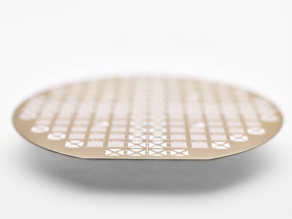
The ready-to-use graphene field effect transistor (GFET) from Graphenea
Could you tell us more about your new GFET product?
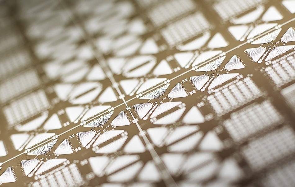
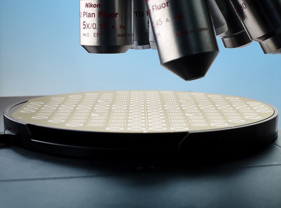
With the GFET, CVD Graphene is transferred onto a silicon wafer that has an insulating layer on top. That graphene is then contacted by metal electrical contacts, and the graphene is patterned into a channel that has dimensions of the order of 10s of microns in size. What that enables you to have is a device where every single carbon atom within the graphene lattice is exposed to the external environment.
The properties of graphene mean that exquisitely small changes in the medium next to the graphene channel cause quite considerable changes in the conductivity of the graphene channel itself. Much more so than the traditional materials that are used in FETs such as silicon. These properties make Graphene FETs very exciting for sensing applications.
Our GFET products are produced using the same high-quality CVD graphene that we've been providing for years and include 36 individual GFETs on a one square centimetre die. Initially, we're launching two variants of this product, the GFET-S10 and GFET-S20, with each having different layouts of the GFETs.
The GFET-S10 has devices distributed evenly over the die and the GFET-S20 has the devices concentrated in the center of the die with the electrical pads located at the edge of the die. It really depends on what the researcher wants to study as to which layout is most suitable, so we’ve tried to have two general layouts to begin with that hopefully satisfy most of the standard requirements of the device researcher.
Can you tell us about other benefits of GFET?
The key thing is the sensitivity of GFETs. The graphene research community has demonstrated staggering results for graphene FET sensors, most strikingly the adsorption of a single gas molecule by a team at the University of Manchester.
However, there are many examples of GFETs being used as an ultra-sensitive transducer whether that be in chemical, bio, or magnetic sensors or photodetectors, and all of these ultrasensitive devices have a common element - the Graphene FET platform. It's that platform that we're launching here and making readily available to the research community.

How will applications such as graphene sensors and R&D benefit from the GFET product?
Fundamentally it's the reduction of the time between the idea and the proof of concept or, putting it another way, lowering the barrier between having an idea and proving the concept. Graphene research has been maturing for 14 years or so now, and a lot of the fundamental science behind the GFETs is largely done, and it's been proven that these Graphene FETs have huge performance advantages over other technologies.
Now it's the time for applied researchers to really exploit these unique properties and develop novel applications or sensors. At the moment, a lot of these applied researchers may be experts in their particular fields - it could be biochemistry for instance - but they're not experts in graphene and in producing graphene devices, both of which are complex areas in themselves.
By launching this product we're hoping to remove the barriers and make extremely high-quality graphene devices immediately available so that researchers can focus on building on top of this very sensitive transducer platform.
Can you tell us about the challenges that these particular applications would have faced without available Graphene FETs?
Many of these sensors are built of two components. They have a transducing element, which is the Graphene FET, as well as a sensitive layer on top, which is sensitive to whatever you're trying to sense; whether it's light, a biochemical species or a particular gas.
Out of those two components, if there was an applied researcher trying to develop a new sensor, then they would have to optimize both components in order to do their research. We're taking one of those components away, so now the researcher can focus on that sensitive layer, which is where a lot of the novelty remains. What is now becoming an established platform is provided by us. Making very high-quality graphene devices is an incredibly challenging thing. It can take years of development on its own to make reliable, high performing GFETs. By providing this product, a researcher doesn't have to do that, and can focus on where the interesting science remains.
There could also be researchers in R&D departments that have a particular technology, and they might be interested in investigating the benefits of graphene devices, but they can't justify a large investment into setting up a new graphene activity. This lowers the barrier to taking steps towards the adoption of graphene within their existing technology platforms.

What benefits are there for researchers working with graphene sensors? Can you tell me about the benefits that they will see from Graphene FET?
First and foremost, I think they have more time to focus on the novel parts of what they're trying to develop, and they can now rely on high quality, reliable supply of GFET devices to work with. Secondly, and just as importantly, we want to work with researchers, the community and R&D departments who might be looking at new graphene applications.
Initially we're going to provide two standard layouts of the GFET. We fully recognize that these are probably not optimal for any particular application, they are general layouts. However we want to work with the researchers and understand what designs are going to meet their needs best. In order to do that well in the coming months, we're going to also launch a custom design service so that researchers can submit their own designs, and that will allow them to tailor the devices to their particular requirements.
So, initially they have a reliable supply, with GFETs to start with and to take them through their initial investigations. We’re then there to support them as their research develops and as they want to further optimize their devices by tailoring the design to what they really need.
Are there any other applications that would benefit from the Graphene FET product? How?
From our understanding the main application currently is in sensing, and in new sensors based on the GFET platform. But there are other exciting opportunities in advanced photonics and electronics, which can benefit from these products.
We want to actively engage with the end users to really understand what their requirements are and to work with them to develop future graphene applications.
What does the Graphene FET product mean for the future?
Some people say graphene has struggled to translate from the fantastic science that's happened in the labs. However, it promises incredible properties and it may have been slow to gain large scale commercial success.
This could be for many reasons. One might be that it takes a substantial investment to start a graphene research activity. Graphene is a complex material and reliably making high-quality devices out of graphene is not a small undertaking.
What we hope the launch of this product does is lower the barrier to investigating how graphene can enhance existing applications, and maybe provide the incremental performance improvement within existing product roadmaps. This would allow graphene to make entrances into relevant markets and create great value.
Where can our readers find out more about Graphenea?
Our website is at www.graphenea.com. You can find technical documentation relating to all the products we’ve talked about on our website. We also welcome any inquiries to our general technical e-mail address which is [email protected] or via our sales email address which is [email protected].
About Richard White

Richard joined Graphenea in 2016 as Business Development Manager for the UK market. He obtained his PhD in Nanotechnology from University of Cambridge in 2008 and subsequently joined Nokia Technologies to work on sensor applications enabled by nanotechnologies.
Richard's work at Nokia led to over 50 patent families with 21 having at least one granted patent and included novel sensors and sensing and computing architectures. His research started with chemical and bio-sensors based on semiconductor nanowires but quickly the unique value of graphene as a sensor material was recognised and his focus shifted to the development of ultrafast humidity sensors based on graphene oxide and to ultrasensitive photodetectors based on graphene FETs.
Disclaimer: The views expressed here are those of the interviewee and do not necessarily represent the views of AZoM.com Limited (T/A) AZoNetwork, the owner and operator of this website. This disclaimer forms part of the Terms and Conditions of use of this website.