All-natural substances are classified into insulators, semiconductors, and metals. The distinction is made based on their electronic band structure since electrons are responsible for the material structure and properties, both physical and electronic.
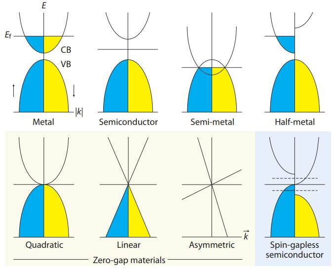
Image Credit: Zero-gap materials for future spintronics, electronics, and optics, X. Wang., et al. University of Wollongong (2010)
Bandgap energy
Semiconductors are materials that have physical properties as defined by their bandgap energy – that is, the energy required to move an electron in the valence to the conduction band.
Electrons have both charge and spin. In traditional electronics, the electronic charge is made use of. However, spin electronics use both charge and spin to process information. Also called spintronics, this branch uses magnetic metals and half-metals, magnetic semiconductors and magnetic insulators which make use of an additional degree of freedom of the electron, in the form of spin. Ferromagnetic and antiferromagnetic semiconductors are the basis of semiconducting spintronics. These rely on the degree to which the free-electron spin is polarized within a material. Complete polarization of the electron is possible with half-metals and some dilute magnetic semiconductors.
Metals have a conduction band which is partially filled so that the Fermi level is present within this band. However, insulators have a large energy gap, separating conduction and valence bands in their structure. Semiconductors have a small energy gap, and half-metals have overlapping conduction and valence bands. In one direction of spin, the half-metal is metallic, while in the other it is semiconducting.
Gapless semiconductors
Gapless semiconductors are a very new class of solids in which the conduction and valence bands meet at the Fermi level. As a result of this structure, the threshold energy needed for electrons to move from occupied states in the valence band to unoccupied energy band levels is zero. This gives them unique abilities. For instance, they are highly sensitive to any external pressure or magnetic field. Their electrons are much more mobile, by 2-4 orders of magnitude than for classical semiconductors.
Some examples include HgCdTe, HgZnSe, and graphene. The zero-gap materials may show energy-momentum dispersions in various forms, namely, quadratic, linear, or asymmetrical. They also exist in various states.
Quadratic dispersion materials
The gapless state may be attained with quadratic dispersion materials by varying the hydrostatic pressure, temperature and other external isotropic effects, affecting the crystal structure. Again, with mercury selenide, in the zero-gap structure, it can be made strongly resistant to magnetization by placing it into a magnetic field parallel to the direction of current flow. The stronger the magnetic field, the more exponentially the magnetoresistance grows. If magnetic ions like manganese or iron are used to dope this material, it becomes greatly magnetoresistant. It is then ideal for use in magnetoelectronics and magnetic field sensors. When pressure is applied, an energy gap appears, and it firstly becomes a semiconductor, then a metal.
Any semiconductor with a narrow energy gap can become a gapless semiconductor if doping is carried out or pressure is applied.
Linear dispersion materials
Graphene is a linear dispersion material, available in a variety of structures. Among these, graphene nanoribbons are unique in achieving single-dimensional gapless dispersions. In graphene, the touching of the conduction and valence bands at some points, making it a gapless semiconductor where the state density vanishes at the Fermi level. As a result, the electron speed is 0.0025 times the speed of light. This is greater than that achieved in any conventional semiconductor. With the nanoribbons, the linear or quadratic form of the dispersion can be regulated by altering the width and chirality of the structure.
The presence of this gapless energy structure for electrons and holes give graphene unique optical characteristics. For instance, it has a nearly constant transmission coefficient between 700-400 nm. For this reason, the excitation of graphene by electrons can allow its electronic properties to be discovered, since almost every optical attribute of an electron and/or hole compound is decided by its optical conductivity.
Other benefits of gapless semiconductors
A gapless semiconductor has optical properties that can be tuned using spintronic effects at low frequencies. The isotropic dispersion of energy around the K point where the two bands touch leads to an optical transition node which can be disabled by spin-orbit coupling, making it possible to increase the total absorption in the terahertz frequency range by 100%.
Gapless states are also closely related to nanomagnetism, whereby, for instance, the gapless dispersion within a graphene nanoribbon splits into magnetic sub-bands. Then the lowest energy state in this system condition will be zero.
Based on this class of materials, researchers are looking into finding novel spin-gapless semiconductors which share many of these advantages, but go far beyond them in extending the range of future applications of these materials. In these materials, the complete spin polarization of both charge carriers (electrons and holes) is possible, and they can be fully separated using the Hall effect. Meanwhile, small external voltages can be used to conveniently manipulate the density and the direction of spin polarization of charge carriers.
Sources
Disclaimer: The views expressed here are those of the author expressed in their private capacity and do not necessarily represent the views of AZoM.com Limited T/A AZoNetwork the owner and operator of this website. This disclaimer forms part of the Terms and conditions of use of this website.