Electron microscopes have played a pivotal role in developing nanotechnologies as their high spatial resolutions make it possible to visualize the smallest of structures. Now, electron microscopy has become a workhorse tool in materials development for both research work as well as manufacturing quality control.
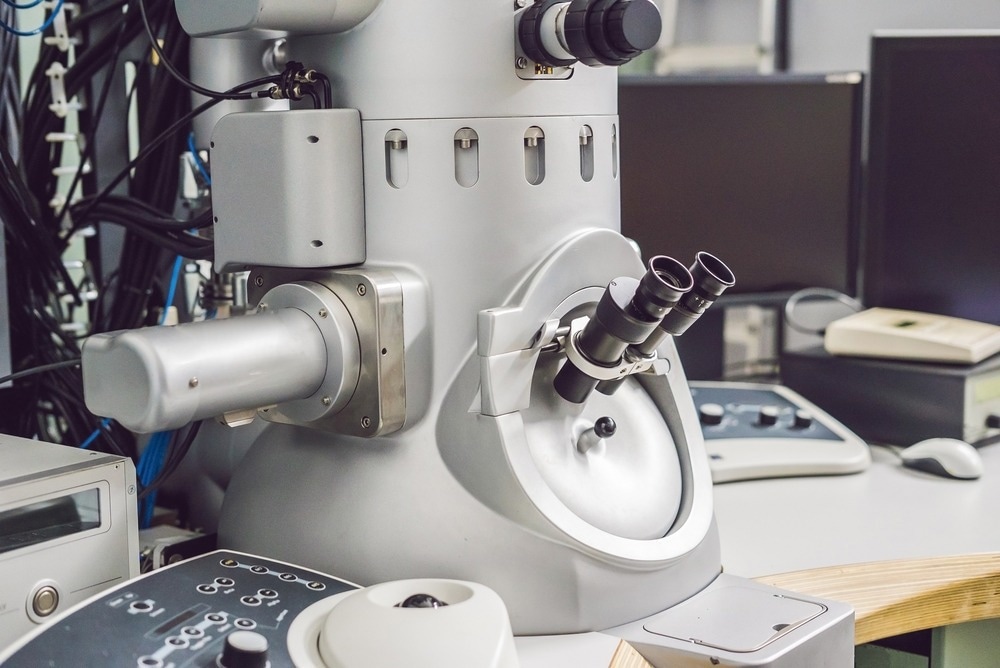
Image Credit: Elizaveta Galitckaia/Shutterstock.com
How are Electron Microscopes Used?
There are a number of electron microscopy techniques, such as cryo-electron microscopy, that are normally used for imaging biological structures. Some of the most widely used electron microscopy techniques include scanning electron microscopy (SEM) and transmission electron microscopy (TEM). Both scanning and tunneling electron microscopy can achieve sub-Angstrom spatial resolutions making them invaluable for nanotechnology applications and capable of single atom imaging.
Electron microscopy can be used to identify both the elemental composition of a nanomaterial as well as its structure. For materials with defects, the elemental and spatial information is particularly valuable from small localized disruption to the overall crystalline order of the material.
Defect sites can be caused by chemical impurities in the processing and contamination of samples but sometimes are intentionally introduced to change the material properties.
Identification of highly localized and small features such as defects is one of the reasons that achieving high spatial resolutions in an electron microscope is so critical.
However, one of the challenges when building an electron microscope is finding ways to control the electron beam. The electron beam needs to be tightly focused on the sample, as the spot size of the beam is linked to the maximum achievable spatial resolution. However, focusing electrons is challenging as they are negatively charged particles. This means that reducing the beam area increases the interaction between the electrons causing stronger repulsion between them, known as space-charge effects. The problem is exacerbated the ‘brighter’ the electron beam, i.e., the higher the electron density.
The brightest electron microscopes make use of lens designs to help control the spatial properties of the beam to maintain small focal spot sizes with high electron densities. Some electron microscopes are even capable of time-resolved imaging, where pulses of electron bunches are used for imaging samples and their time evolution with picosecond or even femtosecond resolution.
Most Powerful Electron Microscopes
An electron microscope consists of an electron source, often called an electron gun, beam handling optics and detector. The exact design of the detection depends on whether measurements are being made in transmission mode, where the beam passes straight through the sample, or the electrons are being scattered from the surface and collected.
The electron lens system is one of the most important parts of an electron microscopy instrument. Whereas the electron gun controls how many electrons will be produced in the instrument and how bright the resulting electron beams will be, the lens system ultimately determines what resolution can be achieved with the instrument and the amount of magnification possible.
Some of the most powerful electron microscopes in the world include the Thermo Fisher ThemIS transmission electron microscope housed at the Lawrence Berkeley Laboratories, the Themis-Z microscope in the University of Sydney and new analysis and instrumentation development at Cornell University that has recently set new records for the level of spatial resolution achievable to 20 picometers.
The ThemIS instruments were already capable of achieving spatial resolutions less than half the width of hydrogen atoms though one of the challenges for electron microscopy is dealing with artifacts in images. The recent developments at Cornell are particularly noteworthy as this development allows for the correction of the aberrations caused by lenses and the problems of multiple scattering from the sample.
Transmission electron microscopy typically uses very thin samples not just because enough of the electron beam needs to pass through the sample that reasonable signal levels can be achieved on the detector but also because the presence of more layers of atoms increases the amount of electron scattering. Correcting for these factors and electron-probe aberrations means the theoretical resolution limits achievable now by many electron microscopy instruments can now be realized in real images.
Another advantage of this development is it allows for imaging of thicker samples. As electron microscopy measurements need to be made in a vacuum, not all materials are capable of withstanding the sample preparation and exposure conditions intact. Being able to use thicker slices makes it easier to prepare samples as they do not need to be sliced with such precision and improves the possibility of the sample remaining undamaged by the microscope environment.
Research Innovations in Electron Microscopes
Electron microscopy instruments have become more commonplace in research and industrial laboratories are their use is likely to continue to increase as instrumentation becomes more affordable.
One of the advantages of electron microscopy over X-rays for structural imaging is that the signals from interaction with the sample tend to be much stronger. However, while brighter and brighter instruments may seem desirable for reducing experimental acquisition times, there is a competing challenge in dealing with sample damage due to the electron beam. Sample damage becomes more problematic as exposure times are longer and electron beams are more intense.
One way to circumvent the sample damage issue and reduce the complexity of electron microscopy measurements and subsequent analysis is to use more sophisticated automated acquisition and analysis programs. Particularly for three-dimensional imaging in scanning electron microscopy, when many layers of images need to be acquired for a full reconstruction, taking the minimal number of slices means less beam exposure time for the sample.
Improvements in autofocusing algorithms and other aberration reduction aids have also meant electron microscopy can move towards being more automated and usable on batches of samples without requiring time-consuming manual reconfiguration between scans.
For nanotechnology, imaging at the atomic level has already been a very real possibility, but improved accessibility of electron microscopy techniques means that it is possible to get a better understanding of the structure-function relationships at this size scale. Many fields, such as nanoplasmonics, rely on physical phenomena that only occur when the length scale of the device is comparable to the wavelength of light being used, and electron microscopy is the tool that makes it possible to visualize and identify these structures.
References and Further Reading
Zhang, N. F., Postek, M. T., Larrabee, R. D., Vladár, A. E., Keery, W. J., & Jones, S. N. 1999. Image sharpness measurement in the scanning electron microscope - Part III. Scanning, 21(4), pp. 246–252. https://doi.org/10.1002/sca.4950210404
Bai, X. chen, McMullan, G., & Scheres, S. H. W. 2015. How cryo-EM is revolutionizing structural biology. Trends in Biochemical Sciences, 40(1), pp. 49–57. https://doi.org/10.1016/j.tibs.2014.10.005
Smith, D. J. 2008. Ultimate resolution in the electron microscope? Materials Today, 11, pp. 30–38. https://doi.org/10.1016/S1369-7021(09)70005-7
Campbell, G. H., Mckeown, J. T., & Santala, M. K. 2014. Time resolved electron microscopy for in situ experiments. Applied Physics Reviews, p. 041101. https://doi.org/10.1063/1.4900509
Chong, L. 2018, There’s a New Microscope in Town, https://newscenter.lbl.gov/2018/06/07/theres-a-new-microscope-in-town-themis-anyone/
Bradley, J. (2018), Australia’s Most Powerful Electron Microscope
Chen, Z., Jiang, Y., Shao, Y., Holtz, M. E., >odsrcil, Guizar-Sciairos, M., Hanke, I., Ganschow, S., Schlom, D. G., & Muller, D. A. 2021. Electron ptychography acehives atomic-resolution limits set by lattice vibrations. Science, 372, pp. 826–831.
Schorb, M., Haberbosch, I., Hagen, W. J. H., Schwab, Y., & Mastronarde, D. N. 2019. Software tools for automated transmission electron microscopy. Nature Methods, 16, pp. 471–477. https://doi.org/10.1038/s41592-019-0396-9
Campbell, G. H., Mckeown, J. T., & Santala, M. K. 2014. Time resolved electron microscopy for in situ experiments Time resolved electron microscopy for in situ experiments. Applied Physics Reviews, p. 041101. https://doi.org/10.1063/1.4900509
Disclaimer: The views expressed here are those of the author expressed in their private capacity and do not necessarily represent the views of AZoM.com Limited T/A AZoNetwork the owner and operator of this website. This disclaimer forms part of the Terms and conditions of use of this website.