In this article, we explore how X-ray diffraction, also known as XRD, can be used to analyze thin films and the benefits of using this technique.
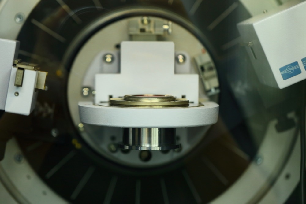
Image Credit: AgriTech/Shutterstock.com
Many materials are now processed in the form of thin films – layers of material that are micrometers or less in thickness. Some films may be as thin as tens of nanometers or even just a single atomic layer of material. The benefits of using thin films in many applications are that they are often easy to process and varying the thickness of the film can be used to tune the material properties, such as the amount of optical absorption.1
Thin films are routinely used in a number of photovoltaic applications, as optoelectronic materials and for specific processes such as water splitting.2 One of the key advantages of thin films is that they can be printed using roll-to-roll printing technologies or through spin coating, and it is possible to make devices that are flexible, lightweight and, in many cases, also retain some degree of transparency.
The development of new materials and devices based on these materials means a need for advanced characterization techniques. In thin film analysis, X-ray diffraction (XRD) is a widely used method for assessing properties such as the degree of crystallinity of the material and its structural characteristics.
XRD is now a widely used analysis technique in many industries, including electronics, materials science and nanotechnology. For very thin films (< 10 nm thickness), many analysis methods can perform poorly, proving problematic for areas such as nanotechnology, where most of the films are have nanoscale thickness. However, the sensitivity of XRD and compatibility with a range of different elements and materials makes it suitable for nanodevices as well as use in other fields.
Principles of XRD
XRD works by illuminating a sample with X-ray light and using a detector to measure the intensity and the angle of the diffracted X-ray radiation. In a crystalline material, the sample will have a periodically repeating lattice structure, and XRD can be used to determine the properties of this lattice experimentally.
Suppose the wavelength of the incident X-rays are tuned to match the periodic spacings in the sample. In that case, some of the incident radiation will diffract at an angle known as the Bragg angle, which is equal to half the angle of the incident radiation. Bragg’s Law states that the angle of incidence of the radiation is equal to the angle of scattering, assuming a condition is met that the pathlength difference between the incident radiation and the periodic material is equal to an incident number of wavelengths.
By measuring the diffraction angle, structural parameters such as the distance between lattice planes and interatomic spacing can be calculated, which make up the periodic unit cell of the material. As long as the diffraction angle is known, a series of known relations, such as the Nelson-Riley or Bradly-Jay functions. These methods work well for a variety of material types.3
Thin Film Preparation and Handling
One of the biggest challenges in thin film preparation is finding ways to achieve uniform thickness when creating the sample. If the sample is inhomogeneous in thickness across the material, the film will have different properties depending on what part of the material the incident light interacts with.
Commonly used sample preparation techniques include sputtering and evaporation, which have to be carried out inside vacuum chambers. Chemical vapor deposition can also be used, as well as spray pyrolysis methods – the choice of technique depends on the thickness of the film being created and how precisely homogenous the coating needs to be.4 Methods like dip and spin coating are usually logistically more straightforward but are a type of bulk coating preparation method.
XRD Instrumentation for Thin Film Analysis
There are now many options for commercial, lab-based instruments for XRD analysis. Several companies sell commercial diffractometers that consist of some X-ray source, normally a type of cathode ray tube, a sample stage and manipulator and a detector – normally a pixel array detector.5 Most XRD set- ups use goniometers for the sample manipulation as this allows for very precise control of the relative orientation of the sample to the X-rays and to scan all the different diffraction angles to recover the full maps.
For certain applications where higher brightness or spatial resolution is required, a synchrotron source has significant advantages over a lab-based X-ray source. Synchrotron sources can generate a much wider range of X-ray energies, including significantly higher X-ray energies and have greater spatial coherence in the beams. For XRD measurements, all of this means faster and better quality data acquisition in comparison to lab experiments. Poorly crystalline samples also tend to suffer from reduced signal levels.
The choice of detector depends somewhat on the quantum efficiency needed. With higher brightness sources, a less efficient detector may be required. Scintillator designs offer very good quantum efficiency, though they often have a slower response, which may be problematic with synchrotron X-ray sources. Semiconductor detectors can offer excellent spatial resolution and high sensitivity but may also be more costly to implement.
Applications of XRD in Thin Film Analysis
XRD is now a standard analysis technique in the preparation and characterization of thin films for a number of industries, including semiconductor manufacturing, thin-film solar cells, and coatings technology. Recent examples of work include characterization of structural parameters and phase identification of colloidal quantum dots where XRD can be used to understand how the synthesis and nucleation processes occur in the quantum dot manufacture and how the presence of particular elements affects the structure and final properties of the materials.6
Challenges and Limitations
Thin films, in particular organic thin films, still pose some challenges for XRD analysis as the amount of scattered signal is reasonably low. Measurement times, particularly on lab-based instruments, can be relatively long when full diffraction maps need to be recorded, and there is always the challenge of the modeling and fitting of the XRD data to reconstruct the sample structure – which is rarely entirely unambiguous.
New generation synchrotron sources coming online will allow for higher brightness, faster measurements, improved spatial coherence and reduced spot sizes, so for even better spatial resolutions and shorter measurement times. Higher brightnesses and more sensitive detection will be key for compensating for the lower scattering cross sections of the light elements to obtain better quality data.
XRD is now a key technique in the characterization of thin films in research and a number of industrial areas, as it allows for precise characterization of the structural properties of such films.
References and Further Reading
Ohring, M. (2001). Materials Science of Thin Films: Depositon and Structure. Elsevier. doi.org/10.1016/B978-0-12-524975-1.X5000-9
Chopra, K. (2012). Thin film device applications. Springer Science & Business Media. doi.org/10.1007/978-1-4613-3682-2
Kalita, P. K. R., et al. (2000). Structural characterization of vacuum evaporated ZnSe thin films. Bulletin of Materials Science, 23(4), pp. 313–317. doi.org/10.1007/BF02720089
Granqvist, C. G. (2012). Solar Energy Materials & Solar Cells Preparation of thin films and nanostructured coatings for clean tech applications : A primer. Solar Energy Materials and Solar Cells, 99, pp. 166–175. doi.org/10.1016/j.solmat.2011.11.048
Bunaciu, A. A., et al. (2015). X-Ray Diffraction : Instrumentation and Applications X-Ray Diffraction : Instrumentation and Applications. Critical Reviews in Analytical Chemistry, 45, pp. 289–299. doi.org/10.1080/10408347.2014.949616
Maity, P., et al. (2021). Role of Cobalt Doping in CdS Quantum Dots for Potential Application in Thin Film Optoelectronic Devices. The Journal of Physical Chemistry C, 125, pp. 2074–2088. doi.org/10.1021/acs.jpcc.0c09358
Disclaimer: The views expressed here are those of the author expressed in their private capacity and do not necessarily represent the views of AZoM.com Limited T/A AZoNetwork the owner and operator of this website. This disclaimer forms part of the Terms and conditions of use of this website.