Engineers from the U.S. Naval Research Laboratory (NRL) have demonstrated the survivability of single walled carbon nanotube transistors (SWCNTs) in adverse space environment.
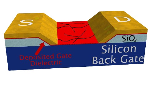
A locally etched back-gated field effect transistor (FET) structure with a deposited dielectric layer. Thick dielectric layers are highly susceptible to radiation induced charge build-up, which is known to cause threshold voltage shifts and increased leakage in metal-oxide semiconductor (MOS) devices. To mitigate these effects, the dielectric layer is locally etched in the active region of the back-gated FET. A gate dielectric material is then deposited (depicted in red) over the entire substrate. (image: U.S. Naval Research Laboratory)
The researchers are exploring ionizing radiation’s impact on the crystalline structures to develop SWCNT-based nanoelectronics that can work under adverse radiation environments. There are two forms of radiation effects, namely transient effects and cumulative effects. Transient effects are single effect transients caused by the generation of a current pulse in a device when an ionizing particle in space directly hits the device. The propagation of this pulse in the circuit results in data corruption, which is disadvantageous to someone relying on that signal, for instance, a user of GPS for navigation.
According to the NRL scientists, such impact is virtually avoided for SWCNT-based nanoelectronics, thanks to their low density, smaller footprint, and inherent isolation from adjacent SWCNTs in a device.
The cumulative effects in conventional electronics are caused by detained charges in the oxides of the devices, such as the gate oxide and oxides used for the isolation of neighboring devices. The latter is the major source of radiation-induced performance deterioration in advanced CMOS devices. The impact becomes evident when there is a change in the voltage required to turn on or off the transistor, first causing power leakage and then ultimately leading to entire circuit failure.
The NRL engineers recently showed SWCNT transistors that survive such radiation-induced performance degradation by designing a SWCNT structure that comprises a thin gate oxide made of thin silicon oxynitride. This combination of the naturally isolated one-dimensional SWCNT structure and the hardened dielectric material makes the SWCNT-based transistors tolerant to both transient and cumulative effects, thus paving the way to develop future space electronics with error-correction circuitry and minimum redundancy, while retaining the same level of fidelity.
This cutback in overhead alone will significantly enhance performance and decrease power over current space-electronic systems albeit the SWCNT-based transistors work at the same speed of existing technologies. It is possible to get more benefits in the future if devices that surpass the performance of silicon-based transistors are developed.
Disclaimer: The views expressed here are those of the author expressed in their private capacity and do not necessarily represent the views of AZoM.com Limited T/A AZoNetwork the owner and operator of this website. This disclaimer forms part of the Terms and conditions of use of this website.