Feb 7 2017
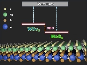 The Anderson model enables a simple way of predicting the offset of the top of the bandgap (labelled as CBO) of 2D semiconductors, such as tungsten diselenide and molybdenum disulfide. Credit: � 2016 KAUST Ming-Hui Chiu
Bandgap is the so-called defining property of a semiconductor, and it is considered to be a barrier that prevents electrons within a particular energy range from passing through a material.
Lance Li, KAUST Professor of Material Science and Engineering, and his team worked together with colleagues from Taiwan and used an easy method to determine the band alignment in an exciting new class of semiconductors known as two-dimensional transition-metal dichalcogenides (TMDs).
The simple concept of bandgap allows a single semiconducting material, such as silicon, to execute the operations needed by electronic devices. However, the device affords a wider range of functionality and possesses enhanced efficiency and performance when two or more semiconductors are combined. Knowledge about how the bandgaps of the two materials align is essential for understanding the behavior of heterostructures.
Even though TMDs and graphene are all atomically thin, the absence of a bandgap in graphene restricts its application to electronics while the existence of a bandgap in TMDs allows them to be stacked in heterostructures. Experimentally determining band alignment between these layers is difficult as the results rely on the quality of delicate TMDs.
Recently, Li and his team proved that the concept called the Anderson model, a computationally inexpensive, simple way of establishing band alignment, is appropriate for this system.
The Anderson model is based on the assumption that when two semiconductors are arranged together, they share a common zero in their energy-band structure called the vacuum level. It is then possible to directly determine bandgap alignment from calculated values of offsets and bandgaps. Until recently, it was not clear whether this assumption would actually hold true in atomic-layer TMDs.
Li and his team addressed this by using the ultraviolet photoelectron spectroscopy method for measuring the energy of the bandgap in three TMDs, tungsten diselenide, tungsten disulfide and molybdenum disulfide. The Anderson model was then used to predict the band alignment. These calculated values were compared with direct experimental measurements obtained from X-ray photoelectron spectroscopy of molybdenum-disulfide–tungsten-disulfide and molybdenum-disulfide–tungsten-diselenide heterostructures.
Agreement between the values derived from the two methods highlighted that the Anderson model holds true. The team pointed out that this is because of unique van der Waals surfaces capable of guaranteeing an absence of dangling atomic bonds that would otherwise put a stop to aligning of the vacuum levels in the two materials.
Our next step is to build heterojunctions based on the knowledge gained from the theory. We will research several heterostructures for various applications, such as solar cells and light-emitting diodes.
Lance Li, Professor, KAUST