Nov 30 2017
Although transistors developed by using carbon nanostructures seem to be a distant dream, they could become reality in the very near future. An international team of scientists in collaboration with Empa has been successful in developing nanotransistors by using graphene ribbons with a width of just few atoms. The study has been published in the latest issue of the Nature Communications journal.
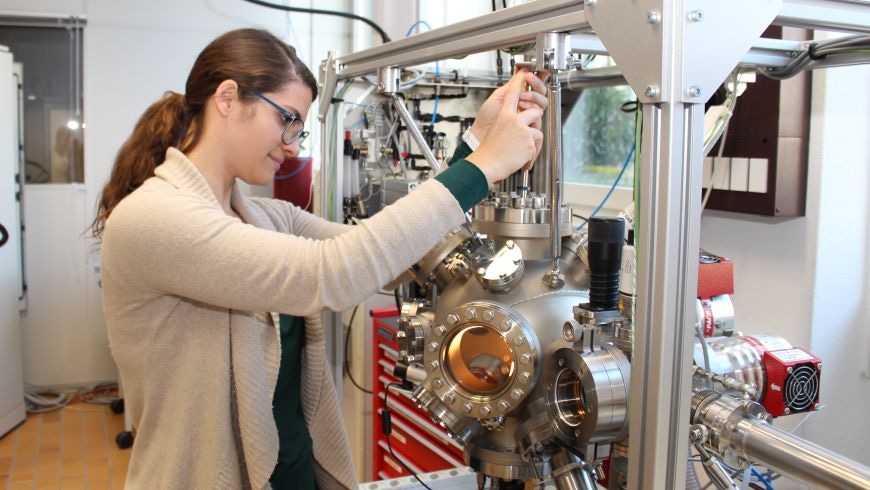 Empa researcher Gabriela Borin Barin evaporates specially prepared molecules in high vacuum to grow graphene nanoribbons. Credit: Empa
Graphene ribbons with a width of just few atoms, or graphene nanoribbons, possess unique electrical characteristics that render them promising for application to nanoelectronics in the future: although graphene, which is a honeycomb-shaped carbon layer with a width of just one atom, is conductive, it can transform into a semiconductor when in the form of nanoribbons. This indicates that graphene includes an adequately large band or energy gap where no electron states can exist—it can be turned on and off and hence can be used as a major component in nanotransistors.
However, even the minute features in the atomic structure of the graphene bands have enormous impacts on the width of the band gap and consequently on the suitability of nanoribbons as transistor components. While the band gap is based on how wide the graphene ribbons are, it is also based on the structure of the edges. As graphene comprises equilateral carbon hexagons, the border might be a zigzag or 'armchair' shape, dependent on the alignment of the ribbons. Although bands that have a zigzag edge act as metals, or conductive, the ones that have the armchair edge behave like semiconductors.
This makes the synthesis of nanoribbons quite difficult because cutting the ribbons from a graphene layer or making them by cutting carbon nanotubes might render the edges to be irregular, so the graphene ribbons might not have the desired electrical characteristics.
Creating a semiconductor with nine atoms
Scientists from Empa partnered with the Max Planck Institute for Polymer Research in Mainz and the University of California at Berkeley to successfully grow ribbons with a width of precisely nine atoms and having a regular armchair edge from precursor molecules. To achieve this, the uniquely synthesized molecules are evaporated in an ultra-high vacuum. At the end of a number of process stages, they are connected similar to puzzle pieces on a gold base to create the desired nanoribbons with a length of nearly 50 nm and a width of about 1 nm.
These structures can be viewed only under a scanning tunneling microscope, and at present have a comparatively large and, moreover, accurately defined energy gap. This allowed the scientists to go one step further and incorporate the graphene ribbons in the nanotransistors. However, at first, their efforts were not fruitful: evaluations indicated that the difference in the current flow for the “ON” state, with applied voltage, and the “OFF” state, without applied voltage, was extremely small. The difficulty was with the dielectric layer of silicon oxide that secures the semiconducting layers with the electrical switch contact. To achieve the desired characteristics, the layer has to have a thickness of 50 nm, which eventually had an impact on the conduct of the electrons.
Yet, the team was then successful in drastically minimizing this layer by applying hafnium oxide, or HfO2, as the dielectric material in the place of silicon oxide. Hence at present, the thickness of the layer is just 1.5 nm and the “on”-current is greater by several orders of magnitudes.
One more challenge was the inclusion of graphene ribbons into the transistor. In the years to come, the ribbons must not be positioned criss-cross on the transistor substrate. In contrast, they have to be aligned precisely along the transistor channel. This will considerably minimize the current high level of non-operative nanotransistors.