Mar 12 2018
Researchers at the Karlsruhe Institute of Technology (KIT) have been successful in observing the growth of very tiny gallium arsenide wires. Apart from providing in-depth knowledge of the growth, the outcomes of their study also enable strategies to produce tailor-made nanowires with distinctive characteristics for specific applications in the future.
Being a semiconductor material, gallium arsenide is broadly used in high-frequency technology for mobile phones, solar cells for space technology, infrared remote controls, and transformation of electric signals into light in glass-fiber cables. The outcomes were reported in the Nano Letters journal by the group of Philipp Schroth of KIT and the University of Siegen.
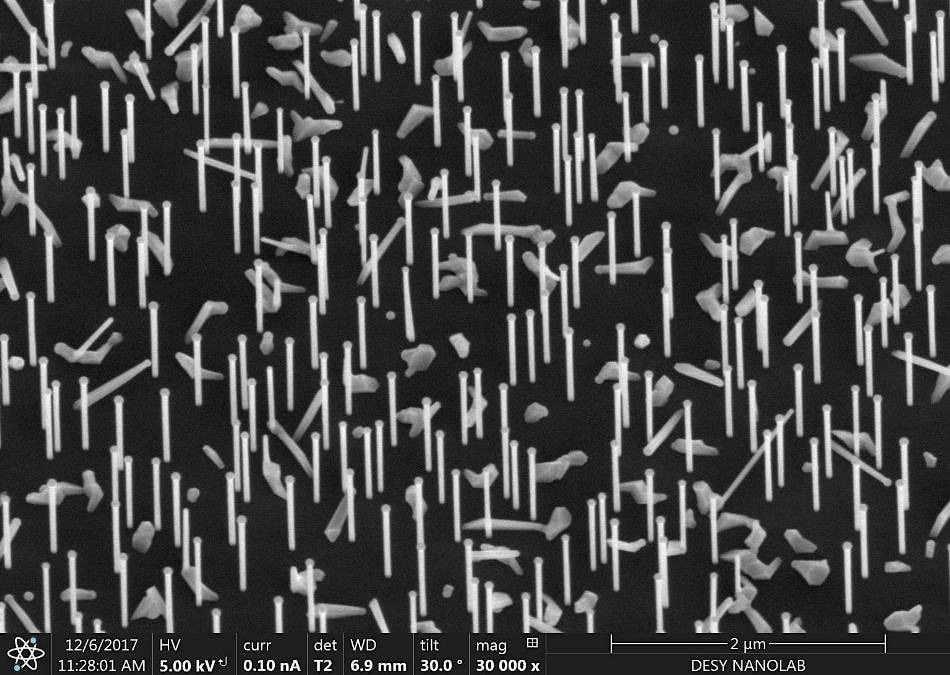 Nanoforest: Nanowires on a silicon wafer as recorded at the DESY NanoLab. (Image credit: DESY, Satishkumar Kulkarni/Thomas Keller)
To produce wires, the researchers adopted the self-catalyzed vapor-liquid-solid process or VLS process. Very tiny liquid gallium droplets are precipitated on a silicon crystal which is at a temperature of about 600 °C. Subsequently, beams of gallium atoms and arsenic molecules are directed at the wafer, where the molecules dissolve in the gallium droplets. After a specific time interval, nanowires start to develop under the droplets, which function as catalysts for the longitudinal growth of the wires.
“This process is quite well established, but it has been impossible so far to specifically control it. To achieve this, the details of growth have to be understood first,” stated Ludwig Feigl from KIT, co-author of the study.
For the investigations, the researchers used a portable chamber particularly developed by KIT’s Institute for Photon Science and Synchrotron Radiation (IPS) with funding from the Federal Ministry of Education and Research (BMBF). The scientists positioned the chamber in the research light source PETRA III of the German Electron Synchrotron (DESY) and captured X-ray pictures every minute to ascertain the diameter and structure of the growing nanowires. At last, they used an electron microscope to evaluate the completely grown nanowires.
We found that growth of nanowires is not only caused by the VLS process, but also by a second component that was observed and quantified directly for the first time in this experiment. This so-called side-wall growth makes the wires gain width.
Philipp Schroth.
During the process of growth of the wires, the size of the gallium droplets increased due to continuous gallium vapor deposition, which has a wide-ranging effect.
“As the droplet size changes, the contact angle between the droplet and the surface of the wires changes as well. In certain cases, this causes the wire to suddenly continue growing with another crystal structure,” stated Feigl.
This transformation is of significance to various applications because the shape and structure of the nanowires have a great deal of impact on the characteristics of the resultant material.