Thin film technology is the process of creating extremely thin layers of material to deposit on the surface of objects ranging from transistors to plate glasses. They are procedures for accumulating and modifying thin coating ranging in thickness from a few nanometres to isolated subatomic levels.
These films are fabricated on platforms by a regulated convergence of ions, micro molecules, and charges, and the procedure is conducted immediately through physical methods or indirectly through electrochemical processes.
Thin films have different optical-mechanical as well as electromagnetic characteristics. Because of these characteristics, they are frequently employed in a variety of industrial applications.
Thin-film sensors are used to measure physical attributes in order to track climatic conditions as well as the variations in any specific environment.
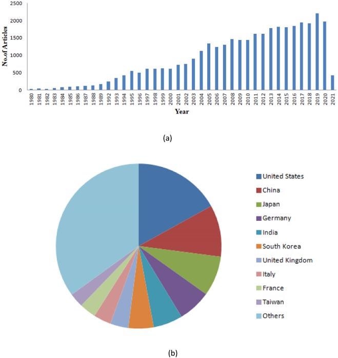
Global trends in Thin film technology: (a) representation of the year-wise publications of research articles that are indexed in the Scopus database. (b) Geographical distribution of patents on thin films. © Elanjeitsenni, V., Vadivu, K. and Prasanth, B., (2022)
Industrial Utilization of Thin Films
Thin films are used primarily in semiconductor technology, electronic components, photovoltaic cells, capacitor, microelectromechanical systems (MEMS), and surface coatings. Thin films of this type are frequently used in optical technology, detectors, medicinal devices, and other applications.
Thin films have recently been employed as detectors for monitoring chemicals, temperature, moisture, stress, substance particles, pressures, and compounds.
Which Substrates are Utilized in Thin Film Technology?
Thin films are often formed on polymer-based, textile-based, and paper-based substrates, as well as nanostructures with complicated topology.
Due to geometrical restrictions, such surfaces have various physical characteristics. Furthermore, macromolecules and nanoparticles may self-assemble into a variety of nanomaterials and patterns. As a result, a variety of cost-effective nanofabrication processes can be designed and employed in a wide range of applications such as nanotechnology and biomedicine.
Famous Polymeric Substrates for Thin-Film Technology
Poly (Ethylene Terephthalate)-PET and Poly (Ethylene Napthalate)-PEN films are polymeric foundations used in the manufacture of thin films. Because of their superior tensile qualities and great resistance to gas and liquid water infiltration, PEN and PET are extensively used in the manufacture of functional devices and solar cells.
Artificially fabricated polymers, such as Polylactic acid (PLA), may be easily modified and utilized as a substrate in thin-film technology.
Biopolymer-based thin films are mostly used in biological applications including tissue regeneration, antifungal coatings, diagnostic devices, and so on.
Paper-based substances also serve as the foundation blocks for electrodes as well as robust energy storage devices such as supercapacitors. Apart from this, researchers have also presented various techniques utilizing inorganic molecules in high stress, and mechanically demanding situations.
Are Conductive Mediums Utilized in Thin Film Technology?
Various conductive media are utilized in the creation of thin films. Metallic nanoparticle ink, which has an excellent electrical conductivity, is the most commonly utilized for making conducting pathways. Inks are further subdivided into single-element metallic nanostructured materials, metallic oxide nanomaterials, hybrid nanocrystals, and core-shell bimetallic nanoparticles (BNP).
Sensor Fabrication Processes
Thin-film sensors are used extensively and are made by different processes each with its advantages and disadvantages. The famous techniques include the sol-gel method, printing methods, sputtering techniques, sintering process, physical vapor deposition (PVD), chemical vapor deposition (CVD), and coating processes such as dip coating and spray coatings.
Deposition techniques and sintering methods are most widely utilized owing to the ease of the process and fast processing.
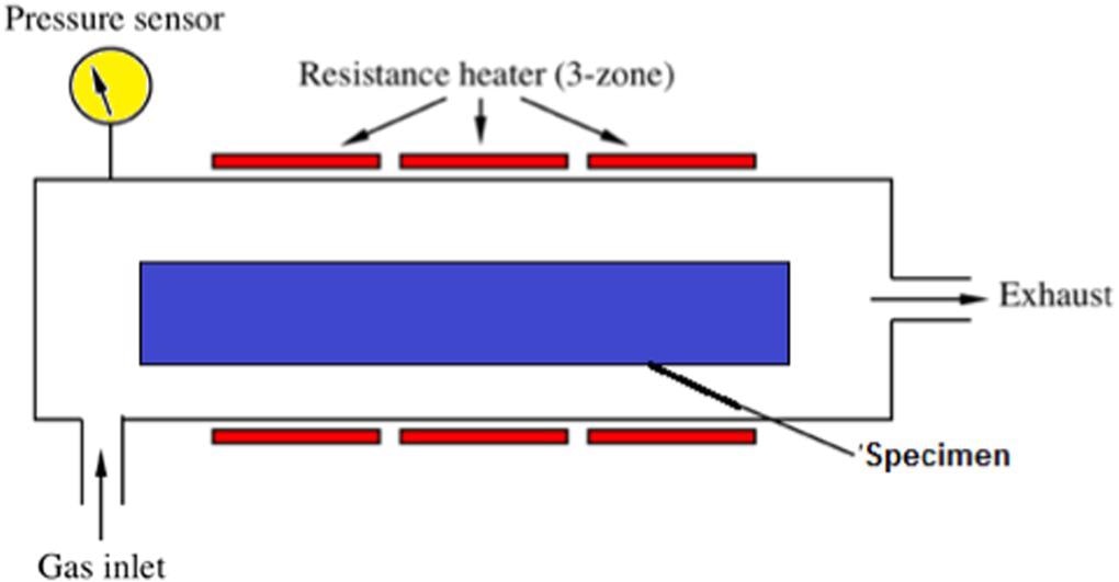
Chemical vapour deposition (CVD). © Elanjeitsenni, V., Vadivu, K. and Prasanth, B., (2022)
Future Perspective of Thin-Film Technology
It should be mentioned that the sintering process, which occurs after the deposition process, is required to improve the conductance of thin coatings. However, because of its elevated temperature, the sintering process is not suited for all materials. Furthermore, greater temperatures result in larger inter-particle necks, which enhances conductivity even further.
After a particular temperature is reached, it causes a drop in conductance owing to the creation of holes. This should be addressed and required further research efforts.
Future studies should concentrate on lowering the processing temperature of the sintering process and manufacturing costs, improving thin-film performance, and producing eco-friendly thin films. This will increase the range of conductive thin film applications.
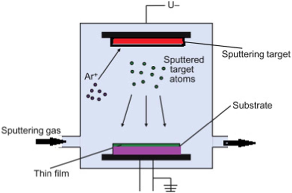
Sputtering of thin films. © Elanjeitsenni, V., Vadivu, K. and Prasanth, B., (2022)
Reference
Elanjeitsenni, V., Vadivu, K. and Prasanth, B., (2022) A review on thin films, conducting polymers as sensor devices. Materials Research Express, 9(2), p.022001. https://iopscience.iop.org/article/10.1088/2053-1591/ac4aa1
Disclaimer: The views expressed here are those of the author expressed in their private capacity and do not necessarily represent the views of AZoM.com Limited T/A AZoNetwork the owner and operator of this website. This disclaimer forms part of the Terms and conditions of use of this website.