Nanometer-scale lateral p-n junctions in graphene represent one of the most promising ways to investigate fundamental quantum phenomena such as Veselago lensing and Andreev reflection.
Realizing nanoarchitectures that can host these properties requires precise control over the size of the lateral p-n junction in the range of nanometer scales is required.
However, realizing clean and sharp interfacial junctions in graphene-based devices has remained challenging until now owing to the inadequate precision of the existing nanolithographic techniques at nanoscales.
Traditional techniques such as local back gating and ion implantation are difficult to implement practically.
Recently, studies related to α-RuCl3/graphene heterostructures have shown that the Dirac-point energy (EDirac) in graphene with underlying α-RuCl3 experiences a massive shift of 0.6 eV owing to the work function-mediated interlayer charge transfer, which is typically greater than 1013 cm-2.
However, the studies have not identified the lateral dimensions of this interlayer charge transfer process. Additionally, the plasmonic behavior of graphene/α-RuCl3 near nanobubbles indicated that the width of the boundaries between pristine and highly-doped graphene is less than 50 nm.
Similar constraints were also observed on the maximum boundary size of lateral charge modulations on the Raman maps of these heterostructures.
In this study, researchers employed a high-resolution local probe to determine the photonic and electronic behavior of nanobubble p-n junctions in α-RuCl3/graphene heterostructure.
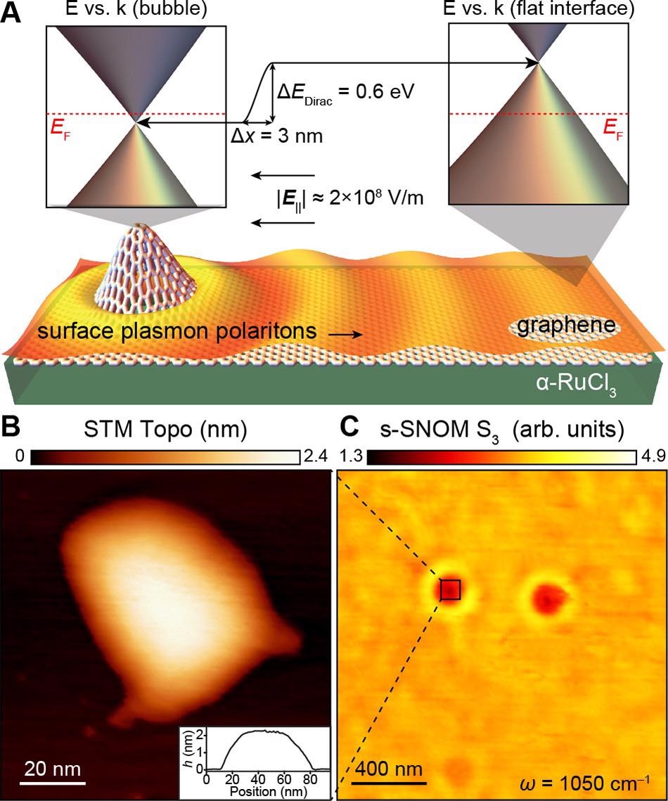
Figure 1. Overview of joint STM/s-SNOM investigation of nanobubbles in graphene/α-RuCl3 heterostructures. (A) Schematic of Dirac-point energy shift between nanobubbles and clean flat interfaces in graphene/α-RuCl3 heterostructures. The ∼0.6 eV energy shift takes place over a lateral length scale of ∼3 nm at the boundary of nanobubbles, generating effective lateral fields of E|| ≈ 2 × 10⁸ V/m (0.2 V/nm). Since the pristine graphene suspended in the nanobubble is intrinsically n-doped, a p–n junction is created at the nanobubble boundary. The associated jump in the graphene conductivity at the perimeter of the nanobubble acts as a hard boundary for reflection of surface plasmon polaritons. (B) Characteristic STM topographic image of a nanobubble (VS = 0.7 V, It = 50 pA). The inset shows the one-dimensional cross section of the nanobubble topography. (C) Characteristic s-SNOM image of two nanobubbles shows circular fringe patterns corresponding to radially propagating surface plasmon polaritons (ω = 990 cm–1). © Rubio, A., Shabani, S., Zhang, J. et al. (2022)
The Study
The αRuCl3/graphene heterostructures were synthesized using dry transfer techniques.
Two complementary spectroscopic and imaging techniques that include scattering-type scanning near-field optical microscopy (s-SNOM) and scanning tunneling microscopy and spectroscopy (STM/STS) were used to understand the intrinsic vertical and lateral length scales of the interlayer charge transfer in α-RuCl3/graphene heterostructures.
Nanobubbles that emerged spontaneously at the interface of the α-RuCl3/graphene heterostructure during fabrication were utilized as a testbed to probe the out-of-plane and in-plane behavior of interlayer charge transfer.
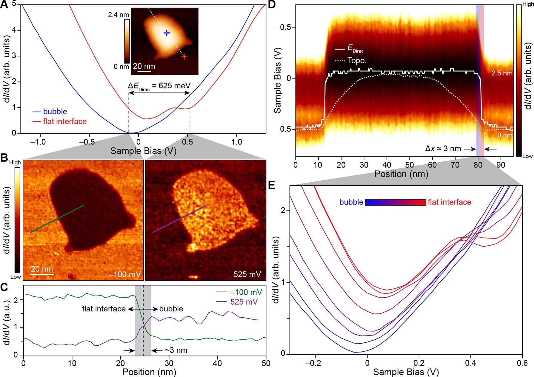
Figure 2. Electronic structure characterization of nanobubbles in graphene/α-RuCl3 using STM and STS. (A) Inset: STM topographic image of a graphene nanobubble (VS = 0.7 V, It = 50 pA). Representative dI/dV point spectroscopy collected over nanobubbles (blue curve) and flat graphene/α-RuCl3 interfaces (red curve) as indicated by the crosshairs in the inset. Between these two spectra, EDirac shifts by 625 meV. (B) dI/dV maps of a graphene nanobubble conducted at the indicated biases corresponding to the Dirac point energies on the nanobubble (left panel) and the flat interface (right panel) (VAC = 25 mV, It = 50 pA). A suppressed LDOS is observed at those biases associated with the local Dirac point energy. (C) Linecuts of the dI/dV maps shown in (B) following the green and purple lines indicated on the −100 and 525 mV maps, respectively. In both instances, the change in the LDOS at the bubble boundary (indicated by the black dashed line) takes place over a lateral length of approximately 3 nm. (D) Position-dependent dI/dV point spectroscopy collected along the dotted white trajectory shown in the inset in (A). The shift in the Dirac point energy occurs over a lateral length scale of ∼3 nm as indicated by the region highlighted in partially transparent red and blue. The position-dependence of the Dirac point energy (solid white line) is superimposed on the topographic line cut (dotted white line) showing that the prior has a much more abrupt spatial dependence than the latter. (E) Sample dI/dV point spectra collected at the threshold of a graphene nanobubble corresponding to the red and blue highlighted region in (D). © Rubio, A., Shabani, S., Zhang, J. et al. (2022)
Observations
The α-RuCl3/graphene heterostructures were fabricated successfully.
The heterostructure comprised large regions of graphene above α-RuCl3. The graphene nanobubbles occasionally interrupted the graphene regions in the heterostructure. The usual heights of the nanobubbles were between 1 and 3 nm, and the radius ranged between 20 and 80 nm.
The near-field signal that was moving radially from nanobubbles displayed an oscillatory nature. The observation was consistent with the presence of surface plasmon polaritons (SPPs) that were either reflected or launched from these nanobubbles.
The spectrum obtained from nanobubbles was almost similar to the spectrum of slightly intrinsically n-doped graphene as the EDirac was located at -100 meV relative to the Fermi energy. This spectrum acted as a reference for the density of states in pristine graphene.
However, the differential conductivity (dI/dV) spectrum obtained from the α-RuCl3/flat graphene region demonstrated a shift in the EDirac to +625 meV relative to the pristine graphene that was suspended in nanobubbles. This significant shift in EDirac corresponded to a hole density of greater than 1013 cm-2 in graphene, which resulted due to the interlayer charge transfer with α-RuCl3.
The local minimum for both spectra was observed close to Fermi energy due to the inelastic tunneling gap.
The gap was emerged owing to the phonon-mediated processes that were independent of the doping level in graphene. This observation of heavily p-doped graphene on the α-RuCl3 surface was consistent with the earlier transport and optical studies and demonstrated the successful formation of p-n junctions at the nanobubble boundaries.
The spectroscopic map associated with the EDirac of nanobubble at -100 mV showed a high local density of states (LDOS) in the area surrounding α-RuCl3/graphene compared to the nanobubble region.
A sharp increase in the LDOS was observed at the boundary between these regions that occurred over a 3 nm lateral length scale, indicating that the nanobubble suppressed LDOS at its EDirac.
However, at the EDirac of α-RuCl3/graphene interface at +525 mV, the LDOS increased in the nanobubble region compared to the α-RuCl3/graphene region.
The local minimum of the Dirac points rapidly shifted at the nanobubble boundary from +525 to −100 mV over a length of a few nanoscales.
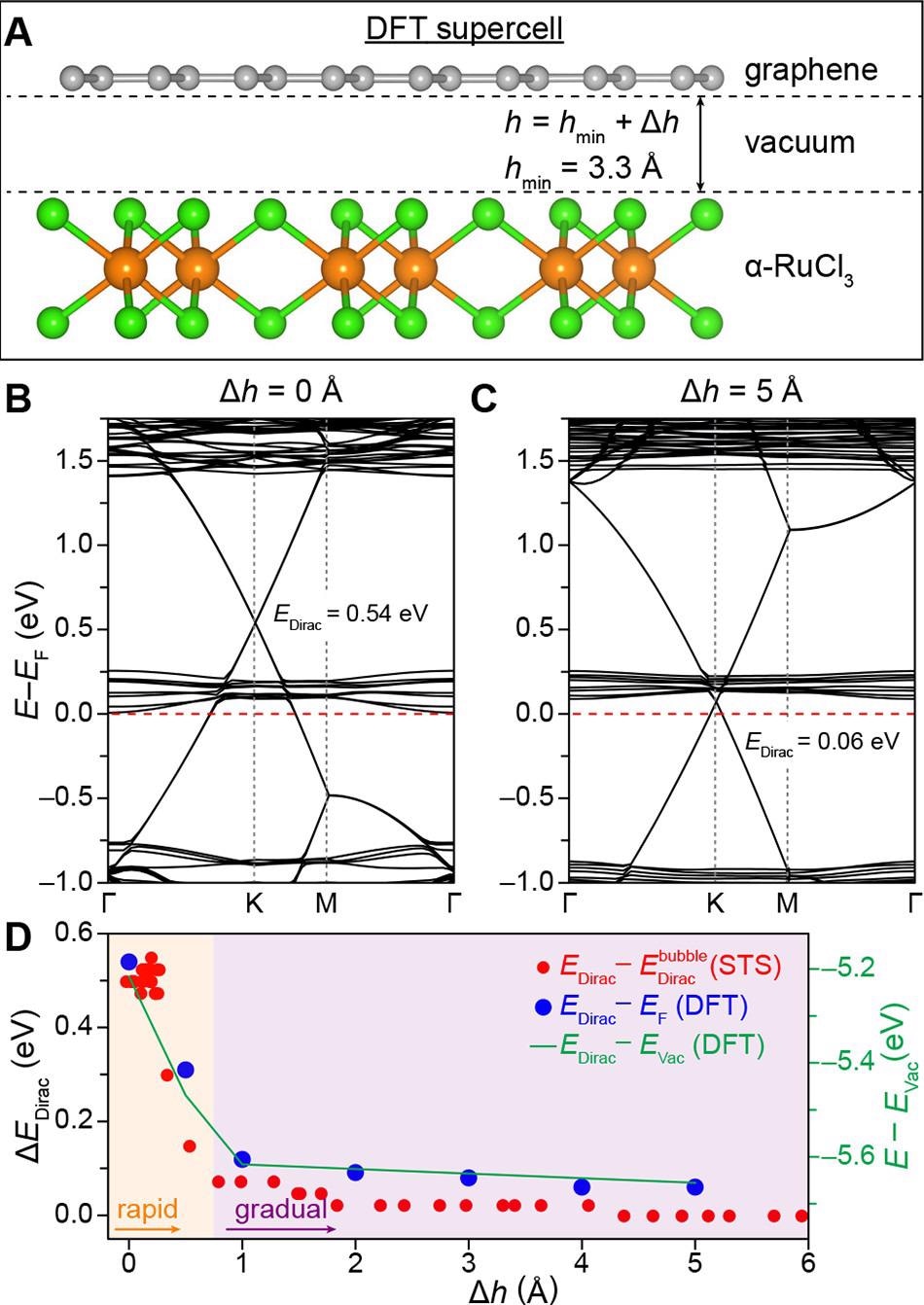
Figure 3. DFT and STM analysis of interlayer charge transfer in graphene/α-RuCl3 heterostructures. (A) Side-view of the graphene/α-RuCl3 heterostructure supercell used in DFT calculations. An equilibrium interlayer separation of hmin = 3.3 Å is used to model the so-called flat interface observed experimentally. To model the charge transfer behavior between graphene and α-RuCl3 at the edge of nanobubbles (where the interlayer separation increases gradually), additional calculations are performed using interlayer separations of Δh = h – hmin = 0.5, 1, 2, 3, 4, and 5 Å. Orange, green, and gray spheres indicate Ru, Cl, and C atoms, respectively. (B) DFT-calculated band structure for a graphene/α-RuCl3 heterostructure with maximal charge transfer (i.e., h = hmin = 3.3 Å). (C) Band structure for graphene/α-RuCl3 heterostructure with h = hmin + 5 Å, showing minimal interlayer charge transfer. The Fermi levels are set to zero in (B,C). (D) The shift in EDirac relative to its value on the nanobubble plotted as a function of interlayer separation is plotted for both experimental (red dots) and theoretical (blue dots) data. The shift in EDirac relative to the vacuum energy EVac is plotted with a green curve. The rapid decay in interlayer charge transfer is highlighted in orange, while the subsequent gradual decay is highlighted in purple. © Rubio, A., Shabani, S., Zhang, J. et al. (2022)
The doping level in the graphene changed more abruptly compared to the nanobubble height profile, indicating that interlayer separation quickly suppressed the interlayer charge transfer.
The intrinsically n-doped and highly p-doped graphene were separated by a 3 nm lateral distance and 0.5 nm vertical distance, which led to the creation of p-n junctions with a band offset of 0.6 eV and generated internal fields on the order of 108 V/m.
The rapid change in conductivity of graphene near the nanobubbles acted as a hard plasmonic barrier that reflected SPPs. Density functional theory (DFT) calculations corroborated the data obtained in this study.
Taken together, the findings of this study provide the conceptual and experimental foundation for generating p-n nanojunctions and validate the effectiveness of using interstitial layers in charge transfer heterostructures to influence the local plasmonic and electronic behavior.
Reference
Rubio, A., Shabani, S., Zhang, J. et al. (2022) Nanometer-Scale Lateral p–n Junctions in Graphene/α-RuCl3 Heterostructures. Nano Letters https://pubs.acs.org/doi/10.1021/acs.nanolett.1c04579
Disclaimer: The views expressed here are those of the author expressed in their private capacity and do not necessarily represent the views of AZoM.com Limited T/A AZoNetwork the owner and operator of this website. This disclaimer forms part of the Terms and conditions of use of this website.