According to the researchers, fascinating developments brought about by curvature at the nanoscale enable them to define a brand-new field called curved nanoelectronics. The origin of curvature effects at the nanoscale is thoroughly examined in this study, along with how they might be used in novel spintronic, superconducting, and electronic devices.
Curved solid-state structures have a wide range of potential applications. Shape changes in electronic nanochannels produce intricate three-dimensional spin textures on a microscopic scale, opening up new possibilities for spin-orbitronics and assisting in the development of energy-efficient electronic devices.
Curvature effects can also encourage the formation of topological insulating phases in semi-metallic nanowires, which can be used in nanodevices crucial to quantum technologies like quantum metrology.
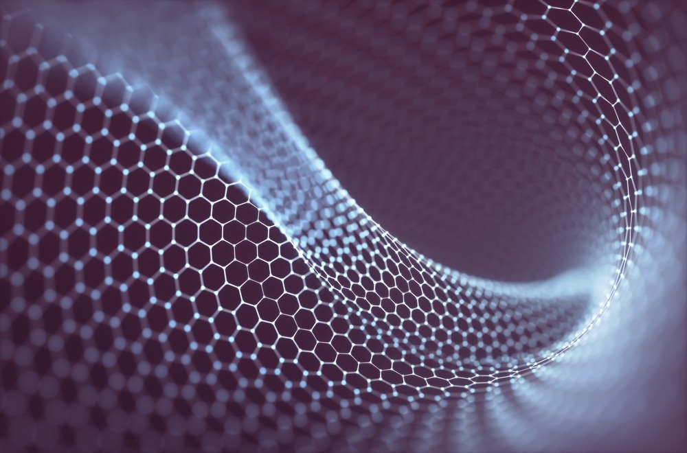 Image Credit: ktsdesign/Shutterstock.com
Curvilinear geometry directly creates the magnetic exchange in the case of magnetism by producing an effective magnetic anisotropy, foreshadowing a significant potential for developing magnetism on demand.
Nanoscale curvature and its associated strain result in remarkable effects in graphene and 2D materials. The development in preparation of high-quality extended thin films, as well as the potential to arbitrarily reshape those architectures after their fabrication, has enabled first experimental insights into how next-generation electronics can be compliant and thus integrable with living matter.
Dr Ivan Vera-Marun, Lecturer, National Graphene Institute, The University of Manchester
The study also identifies key areas for future developments in curved nanoelectronics and discusses the techniques required to create and characterize complex 3D nanoarchitecture, like semiconductor nanomembranes and rolled sandwiches of 2D materials.
Journal Reference:
Gentile, P., et al. (2022) Electronic materials with nanoscale curved geometries. Nature Electronics. doi:10.1038/s41928-022-00820-z.