Electron backscattered diffraction (EBSD) has become a highly popular technique in micro-structural materials characterization. It can be used to determine grain size and grain orientation, in characterizing grain boundaries and in determining texture.
EBSD offers useful insight for a number of different materials and industries, including microelectronics. This article describes the use of Oxford Instruments' AZtecHKL with a Symmetry EBSD detector in the characterization of Through-Silicon Vias, or TSV.
Through-Silicon Vias
TSVs are becoming highly important in the microelectronics industry, due to the continuous demand for faster, cheaper and smaller devices. Typical applications include demanding high power devices, and the integration of many devices on a single package.
Through-Silicon Vias were developed to enable 3D chip integration - the TSVs are used to establish an electrical connection between layers so that the stacked chips function as an integrated circuit.
Performance and Lifetime
This novel technology requires a complete understanding of materials, processes and reliability at the nano-scale. The TSVs are normally formed by etching the silicon - the manufacturing process must be controlled during fast etching so that the TSVs retain a good via profile.
The lining of the etched via is typically an insulating layer of oxide or dielectric, which must maintain its integrity and functionality throughout the device's lifetime.
Failure analysis at this scale typically involves FIB lift-out, followed by analytical and structural characterization in TEM. EBSD offers an SEM-based characterization method that is immediate and effective.
Electron Back-Scattered Diffraction
The main factors influencing TSV performance include the metallic infill structure and the metal-oxide interface.
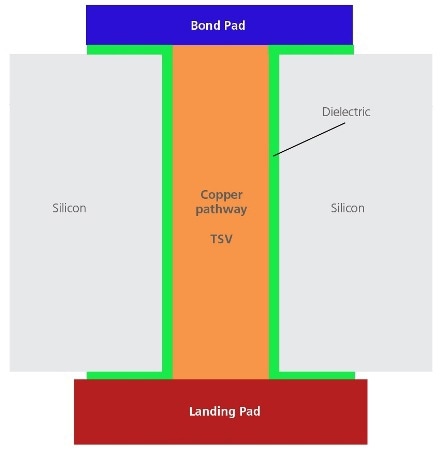
Figure 1. Cross section of silicon wafer showing the TSV - the path connecting two layers.
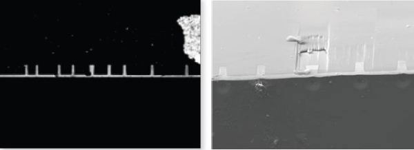
Figure 2. a and b. SEM Backscattered and secondary electron images of the TSVsection.
Grain orientation, grain size and grain boundary types are characteristics of interest. EBSD offers a full characterization of these properties, which is comparable to TEM-based methods. Furthermore, EBSD offers a quantitative description of phases, grain orientation and texture.
Experimental Work
For this study, a TSV sample taken after the filling stage of production was studied. A section of the sample containing a series of TSV's was extracted using a Focused Ion Beam (FIB).
Figures 2a and 2b show this section and the light contrasting vertical features are the TSV's. An ion mill was used to polish this section and the same was examined in a FEG SEM using both EBSD and Energy Dispersive Spectrometry (EDS) techniques. The detectors used included a Symmetry and an X-Max 80 respectively. The EDS and EBSD data was obtained at an SEM acceleration voltage of 20 kV and a probe current of 6.7 nA.
Results
Higher magnification images of the TSV after ion milling are shown in Figures 3a and 3b. The main body of the TSV has a coarse grain structure as shown in Figure 3a). The interface between the silicon substrate is scalloped as in Figure 3b, possibly a result of the etching process. This scalloped region structure differs from the bulk, comprises finer grains and is porous.
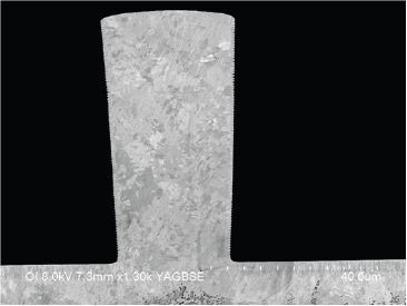
Figure 3a. SEM Backscattered Image (showing atomic number contrast) of the TSV.
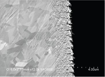
Figure 3b. Higher magnification SEM Backscattered Image of the TSV interface with the silicon substrate. The scalloped region and porosity are seen
Figures 4a to f show simultaneously acquired EBSD and EDS maps. Figures 4a and b shows EBSD pattern quality and phase maps respectively. The pattern quality map offers an overview of crystal structure and the phase map illustrates the spatial distribution of phases identified. The TSV is filled with copper, shown in red, the silicon substrate is blue and there is a region between the copper and the silicon that is un-indexed.
The elements of the substrate and infill are shown in the X-ray maps. The un-indexed region is rich in oxygen and silicon. This oxidized layer produces no EBSD patterns and is amorphous silica. The X-ray map in Figure 4f shows a narrow layer of titanium between the oxygen rich region and the copper TSV, but no EBSD patterns were observed from this titanium layer.
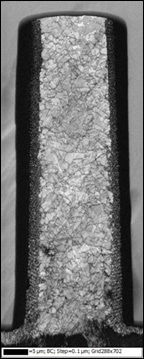
Figure 4a. The pattern quality map illustrates the grain structure within the TSV.
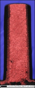
Figure 4b. EBSD phase map: Cu is in red and Si in Blue.
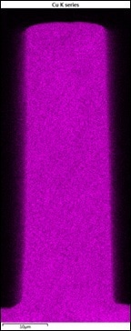
Figure 4c. Cu X-ray map.
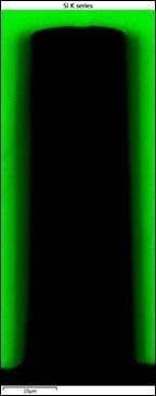
Figure 4d. Si X-ray map.
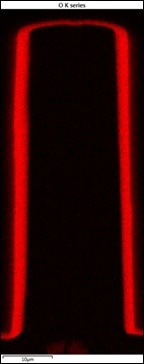
Figure 4e. O X-ray map.
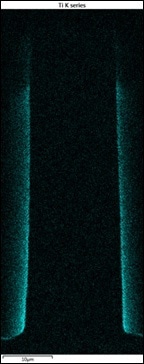
Figure 4f. Ti X-ray map.
Figure 5 shows higher resolution EBSD phase and IPF maps from the TSV/substrate interface. At the interface, the coarse grains within the TSV bulk and the finer grains are clearly seen. A set of pole figures from the surface copper layer, labelled as region A are shown in Figure 6. The pole figures show that the surface copper layer has a very strong <111> fiber texture.
The TSV/ substrate interface is shown at higher magnification in Figure 7. The fine grain structure at the scalloped interface region is clear. These grains also show a strong fiber texture as shown in Figure 7b but with fibre axis <111> rotated about 20 degrees, into the bottom left quadrant of the pole figure.
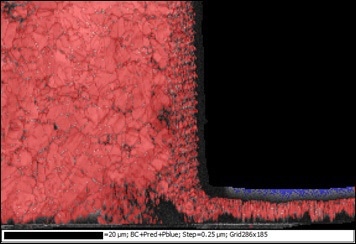
Figure 5a. EBSD Phase Map of the TSV / substrate interface.
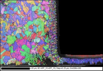
Figure 5b. IPF Map of the TSV / substrate interface.
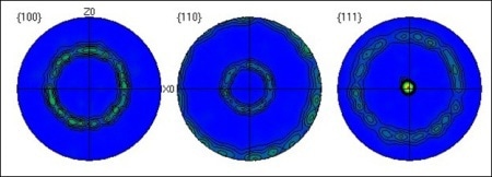
Figure 6. Set of {100}, {110} and {111} pole figures from the copper region A ( Figure 5a).
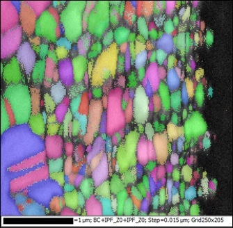
Figure 7a. IPF map from the TSV substrate interface.
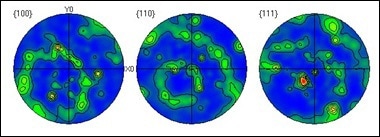
Figure 7b. {100}, {110} and {111} pole figures from the finer grains in Fig. 6a.
Summary
The production process of the TSV is made more clear by the microstructural characterisation using EBSD and EDS.
The TSV had been etched and oxidized to produce an insulating amorphous silica layer, which was then coated with a very thin seed layer of titanium followed by the electro-deposition of copper. The bulk of the TSV has a coarse grain structure, but very fine grains are identified at the interface with the seed layer.
As TSV performance and lifetime is associated with the grain size, grain boundary type and grain orientation, characterizing these parameters during production and in service can provide better understanding for control during production and component lifetime. Microanalysis using EBSD and EDS offers a valuable insight into these key components.

This information has been sourced, reviewed and adapted from materials provided by Oxford Instruments Nanoanalysis.
For more information on this source, please visit Oxford Instruments Nanoanalysis.