Atomic force microscopy (AFM) is an experimental technique that has been embraced in all areas of nanoscience.1 The very high spatial resolutions achievable with AFM, which can be < 1 nm, have enabled the imaging of nanoscale structures and fabrication patterns.2 AFM has become indispensable to the semiconductor industry for both the fabrication and quality control of new semiconductor devices.3

Image Credit: raigvi/Shutterstock.com
Introduction to Electrical Atomic Force Microscopy (AFM)
An AFM instrument uses a probe with an atomically sharp tip to scan over the surface of a material. There are two main scanning modes with an AFM instrument: contact or dynamic (tapping) mode. Both modes differ slightly in how they are performed.
The sharp tip of the AFM probe is attached to a small cantilever that bends when it contacts the surface. The degree of the bend in the cantilever is measured by a highly precise laser and split photodiode, which is a measure of the force being exerted on the tip.
In contact mode, the amount of downward pressure from the instrument on the tip is varied to keep the degree of bend in the cantilever constant. In tapping mode, the tip is raised and lowered near the surface to see what force needs to be applied to make it resonate, and then the amplitude of the tapping motion is kept constant in the scan. This has the advantage of helping to prevent breakage of the fragile tips.
Mapping the amount of force onto the position of the translation stage makes it possible to build up an image of the object being scanned, as the greater the intermolecular interactions from the surface to the tip due to a particular element or raised area, the greater the force applied to the tip.
In AFM, a number of electrical AFM scanning modes are often utilized by the semiconductor industry to understand the properties of materials, such as conductivity or surface potential, as well as the topology of the sample. For such measurements, the tip is coated in an electrically conductive coating.
Examples of electrical AFM scanning modes include conductive-AFM (C-AFM), Kelvin probe force microscopy (KPFM) and piezoelectric force microscopy. (PFM).
Importance of Electrical AFM in the Semiconductor Industry
Electrical AFM is used for a variety of applications in the semiconductor industry, including fault detection and quality inspection of devices. Electrical AFM can also be very useful for analyzing charge distributions in devices and quantitative analysis of the charge levels in different regions of a device.4
The high spatial resolution of electrical AFM means it is possible to check the integrity of the semiconducting material and how structurally and electrically homogenous it is.4
Any small defects or inhomogeneities can lead to later breakdowns of the material and device failure. Often a high degree of sensitivity is required of many electrical AFM scanning techniques to profile semiconductors as the current levels may be too low on the ultra-thin dielectrics used to be detected using other methodologies.
Advantages of Electrical AFM for Semiconductor Characterization
The key advantages of electrical AFM for the semiconductor industry are as follows:
- High degree of spatial accuracy.
- Sensitivity of electrical AFM to site defects in materials.
As semiconductors are moving increasingly towards nanoscale devices, it is important to have analysis techniques capable of resolving structural features on this scale.5
Part of the drive for miniaturization is to allow for enhanced computational power in the same device footprint – where the transistor density is a critical parameter and for an increasing move towards compact, highly energy-efficient devices.
Reduced footprint and energy consumption are necessary not just for increasing the cost-effectiveness of devices or reducing environmental impact but also for enabling remote technologies such as sensing for unmanned aerial vehicles that are used in a number of industries, as well as for climate monitoring.6
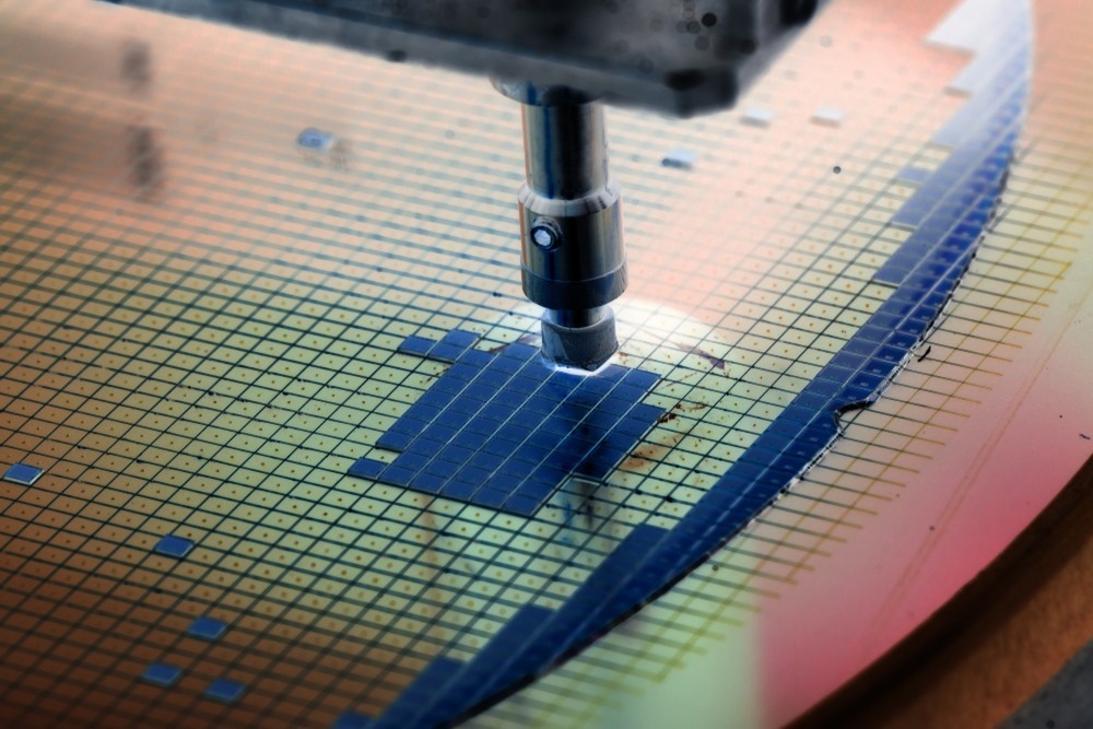
Image Credit: Macro photo/Shutterstock.com
Applications in Semiconductor Research and Development
Some examples of the use of electrical AFM in semiconductor research and development are not just restricted to the more classic inorganic semiconductor devices but are being used for organic semiconductors as well.7 Such research has led to the development of a number of polymer-based or molecular crystal-based devices with excellent performance.8
Other researchers have been using time-resolved AFM measurements to study electromechanical devices and how they work dynamically.9 Such semiconductor devices have properties that are dependent on the amount of mechanical stress on the system. As a result, the forces on the system can be manipulated to tune the resulting electrical properties, which can be characterized by AFM.
Future Trends and Innovations in Electrical AFM
Electrical AFM is now very much a workhorse standard characterization technique for the semiconductor industry, with several commercial solutions available for instrumentation. As miniaturization of devices becomes increasingly common with improvements in the accuracy and affordability of nanoscale fabrication techniques, electrical AFM will become increasingly important as few other techniques can achieve the same degree of spatial resolution in the measurements.
References and Further Reading
- Newberry, D. (2020). Tools Used in Nanoscience. In Nanotechnology Past and Present (pp. 23–32). https://doi.org/10.1007/978-3-031-02084-1_3
- Miller, E. J., Trewby, W., Payam, A. F., Piantanida, L., Cafolla, C., & Voïtchovsky, K. (2016). Sub-nanometer Resolution Imaging with Amplitude-modulation Atomic Force Microscopy in Liquid. December, 1–10. https://doi.org/10.3791/54924
- Shin, C., Kim, K., Kim, J., Ko, W., Yang, Y., Lee, S., … Kim, Y. S. (2013). Fast, exact, and non-destructive diagnoses of contact failures in nanoscale semiconductor device using conductive AFM. Scientific Reports, 3, 1–6. https://doi.org/10.1038/srep02088
- De Wolf, P., Brazel, E., & Erickson, A. (2001). Electrical characterization of semiconductor materials and devices using scanning probe microscopy. Materials Science in Semiconductor Processing, 4(1–3), 71–76. https://doi.org/10.1016/S1369-8001(00)00174-8
- Y, T. (2017). The Role of Nanotechnology in Semiconductor Industry: Review Article. Journal of Materials Science and Nanotechnology, 5(2), 1–10. https://doi.org/10.15744/2348-9812.5.202
- Leuchter, J., Boril, J., & Blasch, E. (2016, September). Practical considerations of SiC technology for UAV. In 2016 IEEE/AIAA 35th Digital Avionics Systems Conference (DASC) (pp. 1-8). IEEE. https://doi.org/10.1109/DASC.2016.7778014
- Zhang, X. Z., Gao, S. J., Qu, Y. J., & Wang, H. T. (2023). Influences of atomic force microscopy probe on the electrical properties of rubrene crystal device. Chinese Journal of Analytical Chemistry, 51(4), 100235. https://doi.org/10.1016/j.cjac.2023.100235
- Rao, V. J., Matthiesen, M., Goetz, K. P., Huck, C., Yim, C., Siris, R., … Zaumseil, J. (2020). AFM-IR and IR-SNOM for the Characterization of Small Molecule Organic Semiconductors. Journal of Physical Chemistry C, 124(9), 5331–5344. https://doi.org/10.1021/acs.jpcc.9b11056
- Calahorra, Y., Kim, W., Vukajlovic-Plestina, J., Fontcuberta I Morral, A., & Kar-Narayan, S. (2020). Time-resolved open-circuit conductive atomic force microscopy for direct electromechanical characterisation. Nanotechnology, 31, 404003. https://doi.org/10.1088/1361-6528/ab9b4b
Disclaimer: The views expressed here are those of the author expressed in their private capacity and do not necessarily represent the views of AZoM.com Limited T/A AZoNetwork the owner and operator of this website. This disclaimer forms part of the Terms and conditions of use of this website.