Silicon wafers are the physical foundation on which virtually every integrated circuit is built. And yet the chain of processes that transforms ordinary quartz sand into a mirror-flat, atomically pure disc, ready to accept billions of transistors, involves more than a dozen precisely sequenced steps, each capable of introducing defects that reduce the number of working chips per wafer.
 Image Credit: asharkyu/Shutterstock.com
This article walks through that chain from start to finish, explaining why each stage exists and where quality is most commonly lost, or won.
Saving this article for later? Grab a PDF here.
From Sand to Metallurgical-Grade Silicon
Silicon is the second most abundant element in Earth’s crust, but is rarely found in pure form. High-purity quartzite (SiO2) is reduced in an electric arc furnace at around 1,800 °C using carbon sources such as coal, yielding metallurgical-grade silicon (MG-Si) at roughly 98-99 % purity.1
For semiconductor use, even a few parts per million of metallic contamination can introduce charge-carrier traps that degrade device performance, so further purification is mandatory.
Purification to Electronic-Grade Silicon: The Siemens Process and Alternatives
The industry workhorse of silicon wafer manufacturing is the Siemens process: MG-Si is converted to trichlorosilane (SiHCl3), fractionally distilled to remove metallic impurities, then redeposited as pure silicon by chemical vapour deposition (CVD) on heated rods.
The result material is polycrystalline silicon, polysilicon, with impurity levels below one part per billion.2
Alternative routes, such as the fluidized-bed reactor (FBR) process, have lower energy consumption and a granular product, though each comes with trade-offs in purity and throughput.
Growing a Single Crystal: Czochralski vs Float-Zone
Logic and memory chips require a single, continuous crystal lattice rather than polysilicon.
The Czochralski (CZ) method dominates large-diameter production: polysilicon is melted in a quartz crucible at ~1,420 °C, and a seed crystal is slowly withdrawn while rotating, forming a cylindrical ingot, or boule, up to 300 mm in diameter.3
An inherent trade-off with the CZ method is oxygen pickup from the crucible walls. In controlled amounts, this oxygen strengthens the wafer but increases metallic impurities; at excess concentrations, it generates electrically active defects that reduce yield.
The float-zone (FZ) method avoids the crucible entirely: a radio-frequency coil moves a narrow molten zone along a polysilicon rod, sweeping impurities to one end. The resulting crystal contains virtually no oxygen, making FZ the preferred substrate for high-resistivity power and detector applications (resistivity exceeding 10 kΩ cm is routinely achieved).1, 3
Surface-tension constraints limit FZ ingots to around 200 mm in diameter, so CZ dominates mainstream logic production while FZ serves specialist markets.
The Silicon Wafer Production Process
Dopant Control and Resistivity Targets
To make silicon useful as a semiconductor, it must be lightly doped with either a Group III element (boron, for p-type) or a Group V element (phosphorus, or arsenic, for n-type).
The dopant is added to the CZ melt or introduced as a gas in FZ growth. Logic wafers typically target 1-50 Ω cm. Power and RF substrates require resistivities several orders of magnitude higher.1
Ingot Shaping and Crystal Orientation
Before slicing, the ingot is ground to a precise diameter, and a flat or notch is added to indicate crystal orientation and dopant type. Orientation matters: (100) wafers are standard for CMOS logic because silicon etches anisotropically, producing clean feature walls, and the Si-SiO2 interface has a lower defect density, improving gate oxide quality. (111) wafers remain in use for bipolar and certain power processes.2, 3
Wafer Slicing with Diamond Wire Saws
The ingot is sliced into wafers using a multi-wire diamond saw, which cuts hundreds of wafers simultaneously.
The process is efficient, but leaves a surface damage layer of crushed and amorphous silicon several micrometres deep, plus measurable thickness variation that must be corrected in later steps.4
Edge Profiling, Lapping, and Damage Removal
The wire saw leaves sharp edges that chip easily, generating particles that contaminate process tools. A diamond wheel rounds these to a standardized profile, reducing stress concentration and improving automated handling.5
Lapping, pressing the wafer between flat plates with abrasive slurry, then removing bulk thickness non-uniformity and saw damage. A follow-up wet chemical etch (hydrofluoric, nitric, and acetic acids) dissolves any remaining subsurface damage, leaving a clean but still hazy surface.
Chemical-Mechanical Polishing (CMP): Achieving a Mirror Finish
CMP is the most precision-critical step in wafer preparation.
The wafer is now pressed against a rotating polyurethane pad wetted with a silica slurry in an alkaline solution. Chemical attack softens a thin surface oxide while mechanical abrasion removes it, producing a planar surface with roughness below a fraction of a nanometre.2
This mirror finish, described as ‘epi-ready’ when clean enough to accept an epitaxial layer directly, is essential for photolithography tools to focus nanometre-scale patterns across the full wafer area.
Ultra-Clean Cleaning and Drying
After polishing, wafers go through wet cleaning sequences, typically modified versions of the RCA clean developed in the 1960s, using sequential chemical baths to lift particles and organics, then strip metallic contaminants.2
Drying uses isopropanol (IPA) vapour or Marangoni methods, which exploit surface tension gradients to remove water without leaving watermark defects on the polished surface.
Final Inspection and Metrology
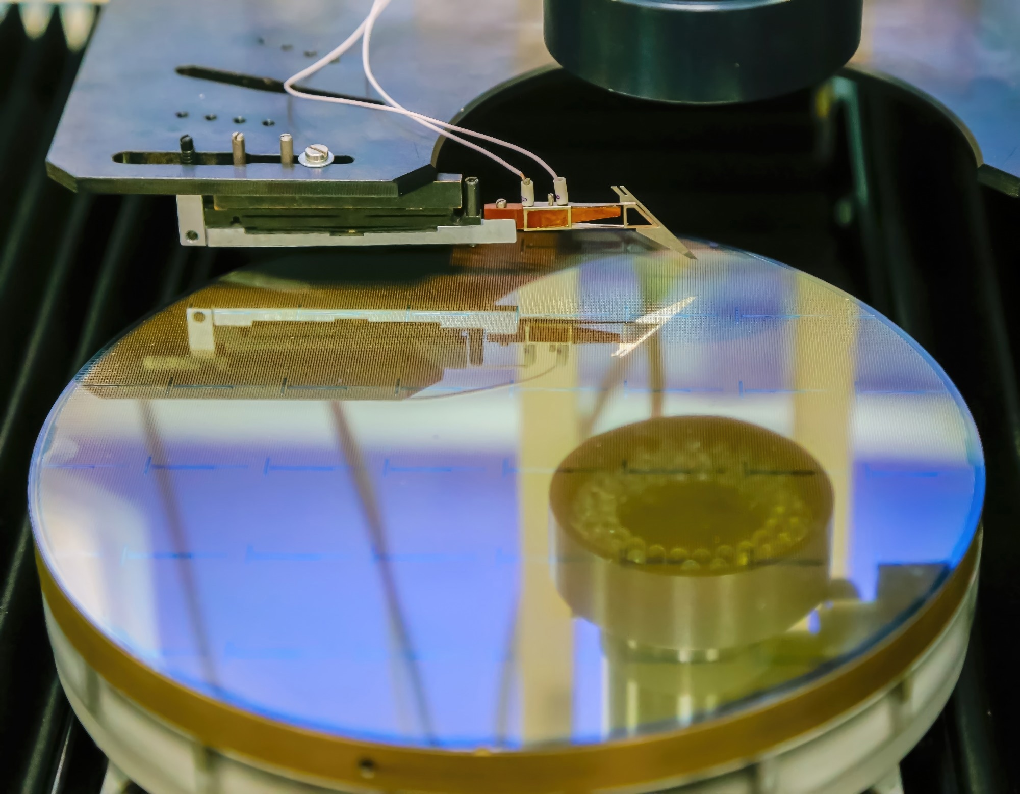 Image Credit: Vital Hil/Shutterstock.com
Each wafer receives a non-contact measurement before shipment.
Total Thickness Variation (TTV) must typically fall below 15 µm on 8-inch prime wafers; advanced nodes demand considerably less.6 Bow and warp, deviations of the wafer’s mid-plane and surface, respectively, affect vacuum chuck behaviour and lithography stage focus.
Surface roughness (measured by AFM) is specified at 0.15 nm Ra or lower for advanced nodes, and laser-based scanners count particles above size thresholds as small as 45 nm.
Resistivity is verified by a four-point probe, and crystal orientation is confirmed by X-ray diffraction. Wafers meeting all parameters are graded ‘prime’; those with looser geometric or cleanliness specs are sold as ‘test’ or ‘monitor’ wafers for process development, where device yield is not the priority.
Why Oxygen, Carbon, and Contamination Control Matter for Yield
Even wafers that pass all geometric checks can fail at the device level due to dissolved impurities. Interstitial oxygen at levels above 14-16 ppma can precipitate during high-temperature anneals, forming bulk microdefects that reduce minority-carrier lifetime. Modern CZ processes target an intermediate oxygen level: enough to gain metal contaminants into the bulk, but low enough to keep the surface device layer clean.1, 2
Carbon, below 0.5 ppma in well-controlled processes, can nucleate these precipitates at lower temperatures. Metallic contamination at even 1010 atoms/cm2 introduces deep-level traps that degrade gate oxide integrity, making contamination control across the entire supply chain as critical as any individual process step.
Outlook and Future Improvements
Crystal growth is perhaps the most important stage: decisions made in the puller, pull rate, melt temperature gradient, rotation speed, and dopant concentration propagate as defects and resistivity non-uniformities into every wafer sliced from that ingot.
Wire-saw slicing and lapping introduce mechanical damage that, if not fully removed, survives into the polished surface as sub-surface cracks invisible to standard optical inspection but detectable under etch.
CMP is where final surface quality is established, and any slurry contamination, pad glazing, or pressure non-uniformity directly affects photolithography performance downstream.
However, contamination control is a continuous thread rather than a discrete step: a single handling event in a poorly maintained cleanroom can deposit enough metallic ions to degrade device performance across an entire lot.
Looking ahead, the industry is actively evaluating 450 mm wafer platforms, which would yield roughly 2.4 times more die area per pull than the current 300 mm standard, though scaling CZ pullers, wire saws, and CMP tools to that diameter introduces fresh engineering challenges at every stage described here.7
References and Further Reading
- FPT Semiconductor. (2024, February 7). A guidance to silicon wafer manufacturing process. https://fpt-semiconductor.com/blogs/a-guidance-to-silicon-wafer-manufacturing-process/
- Elsevier. (n.d.). Silicon wafer. In ScienceDirect topics: Materials science. https://www.sciencedirect.com/topics/materials-science/silicon-wafer
- TRADESAFE. (2024, June 17). Introduction to semiconductor manufacturing: Crystal growth methods. https://trdsf.com/blogs/news/semiconductor-manufacturing-crucial-steps
- Ensoll Tools. (2025, March 28). The complete guide to monocrystalline silicon wafer cutting: Diamond wire saw cutting process. https://www.ensolltools.com/the-complete-guide-to-monocrystalline-silicon-wafer-cutting-diamond-wire-saw-cutting-process/
- Rohm Co., Ltd. (2025, January 16). Evolving semiconductor wafer technology. Rohm TechWeb. https://techweb.rohm.com/trend/glossary/18521/
- Brigham Young University Cleanroom. (n.d.). Wafer specifications: TTV, bow, warp, and defects. https://cleanroom.byu.edu/ew_wafer_specs
- Wang, Y., Li, J., and Zhang, X. (2024). Shaping the future: Innovations in silicon wafer production and finishing. Silicon, 16(8), 6479–6497. https://doi.org/10.1007/s12633-024-03168-5
Disclaimer: The views expressed here are those of the author expressed in their private capacity and do not necessarily represent the views of AZoM.com Limited T/A AZoNetwork the owner and operator of this website. This disclaimer forms part of the Terms and conditions of use of this website.