What is Nanoimprint Lithography?
Process Flow of Nanoimprint Lithography
Tools in Nanoimprint Lithography
Different Types of Nanoimprint Lithography
Applications in Nanoscale Fabrication
Limitations and Challenges
References and Further Reading
Nanoimprint Lithography is a direct mechanical patterning nanoscale fabrication technique, offering high-resolution replication through mold-based deformation of resist materials.
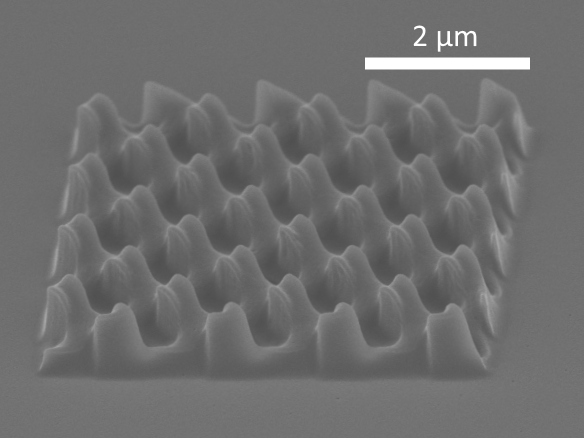 Image Credit: Alexander Koshelev/fiberphotonics.com, CC BY-SA 4.0
What is Nanoimprint Lithography?
Nanoimprint Lithography (NIL) is a nanoscale fabrication technique in which patterns are transferred from a pre-fabricated mold into a deformable resist through direct mechanical contact.
The technique operates through controlled mechanical deformation and interfacial interactions between the mold and resist. Resulting patterns depend on resist rheology, adhesion behavior, and demolding conditions, among other factors.
Unlike conventional photolithography, the process does not require optical or electron-beam exposure. Instead, feature definition is determined by the stamp's geometry - not by light-based resolution limits. This reduces system complexity by removing high-cost optical projection systems and high-energy light sources, lowering both capital and operational costs.
Without being limited by optical diffraction, sub-10 nm feature replication can be achieved, and with high-throughput, scalable manufacturing.
The technique is compatible with a range of diverse substrates, such as:
- Flexible polymers
- Silicon
- Glass
NIL can be used for the fabrication of both planar and three-dimensional nanostructures, making it suitable for applications in electronics, photonics, and microfluidic systems.1,2
Saving this article for later? Download a PDF here.
Process Flow of Nanoimprint Lithography
Mold Preparation
A nanoscale patterned mold is fabricated using high-resolution techniques such as electron-beam lithography.
The mold is a careful reconstruction of the opposite of the desired structure, coated with anti-adhesion layers to enable clean release after imprinting.
Resist Coating
First, a thin polymer resist layer is deposited onto the substrate by spin coating or another similar method. The layer must have uniform thickness to ensure consistent pattern transfer across the entire surface.
Imprinting and Filling
The mold is brought into controlled contact with the resist under applied pressure. The resist flows into the nanoscale cavities through mechanical deformation and capillary action, replicating the mold geometry.
Curing and Mold Separation
The filled resist is then solidified to preserve the imprinted pattern and then carefully detached. This step produces a high-fidelity nanoscale replica on the substrate surface.
Pattern Transfer
The patterned resist layer serves as a functional mask for subsequent processing steps, such as etching, deposition, or ion implantation. It is used to transfer nanoscale features into the underlying material.3,4
Nanoimprint Lithography tools have evolved from modified presses and mask aligners to specialized systems that ensure uniform contact, precise alignment, and controlled demolding.
Full-Wafer and Step-and-Repeat NIL Tools
Modern systems use membrane or roll-based mechanisms that initiate point or line contact before achieving full conformal contact. This minimizes air entrapment and ensures uniform pressure distribution.
Such tools integrate rigid and flexible elements to accommodate surface irregularities while maintaining nanoscale alignment precision below 10 nm over a pressure range from ~10 kPa to 10 MPa.
Jet-and-Flash Imprint Lithography (JFIL) Tools
Jet-and-Flash Imprint Lithography systems are designed for high-throughput fabrication using a step-and-repeat process. Liquid resist is dispensed via inkjet printing, then aligned in the liquid phase, cured with ultraviolet light and then demolded.
These systems use fused silica stamps with engineered flexibility to enable uniform contact, targeting throughput levels above 100 wafers per hour with nanometer-scale alignment accuracy.
Imprint Stamps and Templates
Imprint stamps define nanoscale patterns and are fabricated from materials such as silicon, fused silica, nickel, or elastomers, such as PDMS.
Rigid stamps provide high-resolution patterning but require highly flat substrates, while flexible or hybrid designs improve conformal contact on non-ideal surfaces.
Resist Materials
Resists are the functional layer that captures and transfers the imprinted pattern to the substrate. Thermal resists are thermoplastic polymers that flow under heat and pressure, while UV resists are liquid formulations that solidify through photopolymerization.
Their performance depends on viscosity, polymer chemistry, and additives, while properties such as etch resistance, surface wettability, and mechanical stability determine pattern fidelity and demolding quality.2
Different Types of Nanoimprint Lithography
Thermal Nanoimprint Lithography
Thermal nanoimprint lithography uses a thermoplastic resist heated above its glass transition temperature. Under pressure, the softened material flows into the mold features.
The resist is then cooled before the mold is removed. This method works well, but the heating and cooling steps increase process time.
UV Nanoimprint Lithography
UV nanoimprint lithography uses a low-viscosity liquid resist at room temperature. After the mold contacts the resist and the features fill, ultraviolet exposure cures the material.
Because it avoids full thermal cycling, this version is usually faster and reduces thermal distortion.
Combined Thermal and UV Nanoimprint Lithography
This hybrid approach combines thermal and UV-based curing in one process. It is used to improve dimensional control while reducing mismatch between the mold and substrate.
That can help with large-area uniformity.
Reverse Nanoimprint Lithography
Reverse nanoimprint lithography changes the usual sequence by coating the resist onto the mold instead of the substrate. The patterned material is then transferred to the target surface.
This can simplify the fabrication of some three-dimensional and multilayer structures, especially in photonics and microfluidics.2,5
Learn more about lithography here
Applications in Nanoscale Fabrication
High-Density Data Storage (Bit Patterned Media)
Nanoscale imprinting enables the fabrication of ultrahigh-density bit-patterned media with sub-10 nm features required for next-generation magnetic storage systems. This approach supports replication of highly ordered nanopatterns over large areas with consistent geometry.
Integration with directed self-assembly techniques further improves pattern regularity and reduces defect propagation during scaling.
These capabilities collectively support storage densities beyond conventional lithographic and magnetic recording limits.
Semiconductor Device Fabrication
Step-and-repeat imprinting is used for nanoscale pattern definition during the fabrication of logic and memory devices. The approach reduces dependence on complex optical projection systems while maintaining high-resolution pattern transfer capability.
Scalable processing with controlled defect density enables compatibility with advanced device architectures. This positions imprint-based methods as a potential complementary route in semiconductor manufacturing.
Optical Nanostructures and Photonic Devices
Large-area periodic nanostructures, such as gratings, metasurfaces, and diffractive optical elements, are produced by direct pattern replication. These structures enable precise control over light propagation, diffraction, and polarization.
Compared with serial writing techniques, imprinting offers higher throughput and improved scalability for optical surfaces. Such capabilities are widely used in imaging, sensing, and integrated photonic systems.
Microlens Arrays and 3D Optical Components
Direct mechanical replication enables the formation of complex three-dimensional optical structures in a single imprint step.
Microlens arrays, microprisms, and blazed gratings can be fabricated with controlled geometry and spatial variation. This eliminates dependence on surface-tension-driven processes and expands material selection options. The approach enables scalable production of compact, integrated optical components.
Flexible and Large-Area Electronics
Roll-based imprint processes support the fabrication of electronic structures on flexible polymer substrates. Thin-film transistors, and conductive patterns can be produced using continuous high-throughput methods. This enables integration into wearable devices, flexible displays, and lightweight sensing platforms.
Mechanical compatibility with non-rigid substrates makes the technique suitable for emerging large-area electronics.1,6
Table 1: Applications and benefits of Nanoimprint Lithography (NIL)
| Application |
Why NIL is useful |
| Data storage |
It can replicate very small, highly ordered patterns over large areas, which is useful for bit-patterned media. |
| Semiconductor fabrication |
It offers high-resolution patterning without relying on complex optical projection systems, making it a useful complementary method for some device structures. |
| Optical and photonic devices |
It works well for gratings, metasurfaces, and other periodic nanostructures that need precise geometry over large areas. |
| Microlens arrays and 3D optical components |
It can form complex three-dimensional optical features in a single step, which helps simplify fabrication. |
| Flexible and large-area electronics |
Roll-based NIL can pattern structures on flexible polymer substrates, supporting wearable devices, flexible displays, and lightweight sensors. |
Limitations and Challenges
Nanoimprint lithography also has clear limitations.
Because the mold touches the resist directly, any defect in the mold can be copied into the final structure. Mold wear can also become a problem over repeated use.
Alignment is another challenge, especially for multilayer fabrication. Without the most advanced optical alignment systems, maintaining stable overlay across layers can be difficult.
Other problems come from substrate non-uniformity, environmental sensitivity, and material trade-offs. Softer resists may deform too easily, while harder materials can increase the risk of damage during imprinting or release.4,7,8
Practical Route to High-Resolution
Nanoimprint lithography is a practical route to high-resolution nanoscale patterning without relying on complex optical exposure systems.
Its value is strongest in applications where direct replication, small feature size, and scalable processing are more important than the flexibility of conventional lithography.
References and Further Reading
- Barcelo, S., & Li, Z. (2016). Nanoimprint lithography for nanodevice fabrication. Nano Convergence, 3(1). DOI:10.1186/s40580-016-0081-y, https://nanoconvergencejournal.springeropen.com/articles/10.1186/s40580-016-0081-y
- Schift, H. (2025). Nanoimprint - Mo(o)re than Lithography. Encyclopedia, 5(4), 197. DOI:10.3390/encyclopedia5040197, https://www.mdpi.com/2673-8392/5/4/197
- Torii, H., Hiura, M., Takabayashi, Y., Kimura, A., Suzaki, Y., Ito, T., Yamamoto, K., Choi, B. J., & Estrada, T. (2022). Nanoimprint lithography: today and tomorrow. Novel Patterning Technologies 2022, 1. DOI:10.1117/12.2615740, https://www.spiedigitallibrary.org/conference-proceedings-of-spie/12053/1205301/Nanoimprint-lithography--today-and-tomorrow/10.1117/12.2615740.full
- Cao, Y., Ma, D., Li, H., Cui, G., Zhang, J., & Yang, Z. (2025). Review of Industrialization Development of Nanoimprint Lithography Technology. Chips, 4(1), 10. DOI:10.3390/chips4010010, https://www.mdpi.com/2674-0729/4/1/10
- Lan, H., & Ding, Y. (2010). Nanoimprint Lithography. In Lithography. InTech. DOI:10.5772/8189, https://www.intechopen.com/chapters/16684
- Maruyama, N., Sato, K., Suzaki, Y., Jimbo, S., Yamashita, I., Yamamoto, K., Yamamoto, K., Hiura, M., & Takabayashi, Y. (2023). Advances and applications in nanoimprint lithography. Novel Patterning Technologies 2023, 18. DOI:10.1117/12.2658127, https://www.spiedigitallibrary.org/conference-proceedings-of-spie/12498/124980I/Advances-and-applications-in-nanoimprint-lithography/10.1117/12.2658127.full
- Zhou, W. (2013). Nanoimprint Lithography: An Enabling Process for Nanofabrication. SpringerLink. DOI:10.1007/978-3-642-34428-2, https://link.springer.com/book/10.1007/978-3-642-34428-2
- Raza, A., Saeed, Z., Aslam, A., Nizami, S. M., Habib, K., & Malik, A. N. (2024). Advances, Application and Challenges of Lithography Techniques. 2024 5Th International Conference on Advancements in Computational Sciences (ICACS), 1–6. DOI:10.1109/ICACS60934.2024.10473245, https://ieeexplore.ieee.org/document/10473245
Disclaimer: The views expressed here are those of the author expressed in their private capacity and do not necessarily represent the views of AZoM.com Limited T/A AZoNetwork the owner and operator of this website. This disclaimer forms part of the Terms and conditions of use of this website.