IMEC, Europe's leading independent nanoelectronics research institute, reports a method to integrate high-speed CMOS electronics and nanophotonic circuitry based on plasmonic effects. Metal-based nanophotonics (plasmonics) can squeeze light into nanoscale structures that are much smaller than conventional optic components. Plasmonic technology, today still in an experimental stage, has the potential to be used in future applications such as nanoscale optical interconnects for high performance computer chips, extremely sensitive (bio)molecular sensors, and highly efficient thin-film solar cells. IMEC's results are published in the May issue of Nature Photonics.
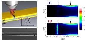 Top left: schematic overview of the device, showing focused illumination of a slit in the waveguide using polarized light. This results in plasmon excitation of the waveguide for the red polarization and the generation of electron/hole pairs in the semiconductor. Bottom left: SEM picture of a typical device. Top/bottom right: Photocurrent scans for the “red” (bottom) and “blue” (top) polarization indicate a strong polarization dependence of the photoresponse – doi:10.1038/nphoton.2009.47
The optical properties of nanostructured (noble) metals show great promise for use in nanophotonic applications. When such nanostructures are illuminated with visible to near-infrared light, the excitation of collective oscillations of conduction electrons – called surface plasmons – generates strong optical resonances. Moreover, surface plasmons are capable of capturing, guiding, and focusing electromagnetic energy in deep-subwavelength length-scales, i.e. smaller than the diffraction limit of the light. This is unlike conventional dielectric optical waveguides, which are limited by the wavelength of the light, and which therefore cannot be scaled down to tens of nanometers, which is the dimension of the components on today's nanoelectronic ICs.
Nanoscale plasmonic circuits would allow massive parallel routing of optical information on ICs. But eventually that high-bandwidth optical information has to be converted to electrical signals. To make such ICs that combine high-speed CMOS electronics and plasmonic circuitry, efficient and fast interfacing components are needed that couple the signals from plasmon waveguides to electrical devices.
As an important stepping stone to such components, IMEC has now demonstrated integrated electrical detection of highly confined short-wavelength surface plasmon polaritons in metal-dielectric-metal plasmon waveguides. The detection was done by embedding a photodetector in a metal plasmon waveguide. Because the waveguide and the photodetector have the same nanoscale dimensions, there is an efficient coupling of the surface plasmons into the photodetector and an ultrafast response. IMEC has set up a number of experiments that unambiguously demonstrate this electrical detection. The strong measured polarization dependence, the experimentally obtained influence of the waveguide length and the measured spectral response are all in line with theoretical expectations, obtained from finite element and finite-difference-time-domain calculations. These results pave the way for the integration of nanoscale plasmonic circuitry and high-speed electronics.