Nov 19 2009
Toshiba Corporation today announced that it has developed a high resolution photoresist (photo-sensitive film) essential for future application of EUV (extreme ultraviolet) lithography in semiconductor fabrication, and proved its viability with the world's first 20nm-scale generation process technology.
This achievement will be announced at 22nd International Microprocesses and Nanotechnology Conference on November 19.
As semiconductor process technology advances and wiring densities get even higher, use of conventional polymer photoresists—the base materials for conventional semiconductor resist—will face hurdles. By the time lithography technology advances into the 20nm-scale generation, use of today's argon fluoride laser exposure apparatus and polymer photoresists will result in difficulties in achieving required resolutions. The solution lies in a transition to EUV lithography and photoresist based on low molecular materials.
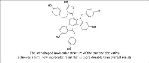
Semiconductor circuit patterning requires photoresists that can be used in both positive-tone and negative-tone processes to secure precise structuring. Toshiba has developed a low molecular resist for EUV generation by employing a derivative of truxene, a low molecular material that is finer and more durable than currently used polymer materials. The company applied this resist to positive tone process, and has now succeeded in applying it to the more demanding task of the negative tone process and forming a test pattern in the 20nm-scale generation.
Toshiba will further improve the performance of the molecular resist and apply it to the fabrication of 20nm-scale generation LSIs. According to the International Technology Roadmap for Semiconductors (ITRS), high volume production of this generation is expected to start in 2013.
When semiconductors circuit patterns scale down into the 20nm-scale generation, current photoresists will no longer resolve circuit patterns precisely, resulting in roughness in pattern sidewalls. The biggest factor is that conventional photoresists consist of polymer compounds. While such compounds are easier to spin-cast on wafers, the size of their molecules and entangling of their molecular chains limit resolution. To overcome this, Toshiba has developed a photoresist with smaller molecular compounds.
Once a photoresist is exposed to light, it is removed from the substrate with a developer solution in one of two ways, positive tone and negative tone. In positive-tone development, the area exposed to the light source is removed from the wafer (i.e. that part of the photoresist becomes more soluble), leaving a channel. In negative-tone development, the area that has not been exposed to the light source is removed from the wafer (i.e, that part of the photoresist becomes more soluble), leaving a raised area. Application of both processes is essential for etching wafers.