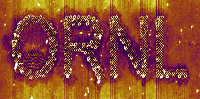
Researchers at Oak Ridge National Laboratory (ORNL) have successfully carved out nanoscale designs on polymer surfaces using atomic force microscopy (AFM).
The nanofabrication was performed on a substrate made from a new class of ionic polymer materials. This study demonstrates that the nanostructures required for increasingly smaller electronic devices could be fabricated using AFM.
“Right now the size of the formed features is in the range of 100 nanometers, but it’s not the limit. We believe it’s possible to change the experimental setup to advance to lower scales.”
Vera Bocharova
 Oak Ridge National Laboratory researchers used atomic force microscopy to draw nanoscale patterns in a polymerized ionic liquid.
Polymers from ionic liquids
Ionic liquids have been the subject of research for several years. They are essentially organic salts which are typically liquid at room temperature - their conductivity and unusual properties have led to suggested applications in batteries, and as solvents for low temperature chemical synthesis.
More recently, polymerized ionic liquids have been found to have equally fascinating properties. These materials have a unique structure, and demonstrate high ionic conductivity. They expected to have applications in lithium batteries, solar cells and transistor technologies. However, since they are still relatively new, many properties of these materials have not yet been fully explored.
Surprise results
ORNL researchers conducted experiments to characterize the properties of polymerized ionic liquid thin films using AFM. They were surprised with the results:
“We were expecting to measure ionic conductivity, and instead we found that we were forming holes on the surface. Then we started to think about how this might have great applications in nanofabrication.”
Vera Bocharova, corresponding author
Nanoelectronic potential
Nanolithography is a widely used technique for nanofabrication; however, it has size limitations. The increasing demand from the semiconductor industry for nanoscale features smaller than traditional lithography techniques can achieve has led to a huge amount of research into other potential methods. One of the possibilities that has been discussed is using AFM to etch nanoscale patterns into a surface.
AFM techniques similar to the one used at ORNL have been used for making patterns in nonconductive polymers. However, the ORNL study demonstrated a number of benefits to using polymerized ionic liquids in this context. Bocharova commented:
“In comparison to nonconductive polymers, we have to apply less bias — four volts instead of 20 volts — to generate the holes, which is good in terms of energy savings for future applications.”
When a high voltage is applied to nonconductive polymers through the tip of an AFM, the material’s surface gets punctured due to localized heating. In the ORNL study, when the researchers investigated what was happening, they found that the holes in the conductive polymers were formed due to the migration of negative ions to the positively charged microscope tip.
The team of researchers now intends to develop this technique further, and expand their knowledge about the properties of polymerized ionic liquids.
The other coauthors of this study are ORNL’s Alexander Agapov, Alexander Kisliuk, Alexander Tselev, Alexei Sokolov, Bobby Sumpter, Evgheni Strelcov, Ivan Kravchenko, Rajeev Kumar, Sergei Kalinin; Veronika Strehmel and Stefan Berdzinski of the Hochschule Niederrhein University of Applied Sciences; and Liam Collins of the University College Dublin. An ORNL-University of Tennessee Governor’s Chair appointment is held by Sokolov.
ORNL’s Laboratory Directed Research and Development program has provided support for this study. The National Science Foundation and DOE’s Office of Science have provided support for certain parts of the study. Some part of the research was conducted at ORNL’s Center for Nanophase Materials Sciences.
Sources and further reading