Researchers redesign the synthesis surface to address a key challenge in DNA data storage: shrinking writing sites without sacrificing DNA yield.
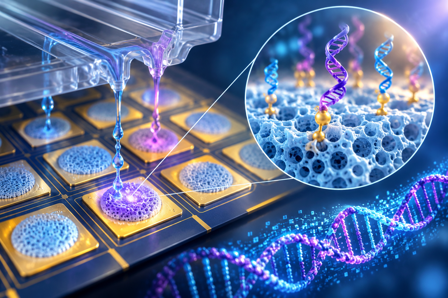
Paper: Enhanced electrochemically-directed oligonucleotide synthesis via porous silica thin-film for DNA data storage. AI-generated abstract conceptual image created using ChatGPT/OpenAI
A recent paper in Microsystems & Nanoengineering reported improved electrochemically directed synthesis (EDS) of oligonucleotides for deoxyribonucleic acid (DNA) data storage using a porous silica thin film.
DNA data storage
Under proper conditions, DNA can preserve data over millennial timescales and offers extremely high theoretical storage density, making it a promising medium for long-term cold-data storage.
Digital data is encoded into nucleotide sequences, and the corresponding oligonucleotides are physically synthesized to write the information into DNA.
On-chip oligonucleotide synthesis performs reactions in parallel across large arrays, increasing writing throughput compared with conventional phosphoramidite-based column synthesis.
Importance of EDS
EDS suits highly integrated DNA writing because it is compatible with electrical addressing and standard microfabrication methods. Microelectrode arrays generate acid locally for spatially selective deblocking, enabling addressable, programmable parallel synthesis. Deblocking removes a protective chemical group, allowing the next nucleotide to be added.
EDS platforms have reached synthesis-site densities approaching 107 sites/cm² by shrinking individual electrode features, showing their potential for high-throughput DNA synthesis.
Yet continued miniaturization reduces the available reaction surface and the number of molecular copies produced at each site, creating a trade-off between per-site oligonucleotide yield and synthesis-site density. Low molecular copy numbers can compromise reliable data recovery.
The role of silica
Silica nanoparticles (NPs) are attractive solid-phase supports for oligonucleotide synthesis because they offer high specific surface area, chemical stability, and readily functionalizable surfaces.
Yet densely packed NP assemblies can form irregular, poorly interconnected pore networks that restrict reagent transport and reduce access to internal reactive sites. Small or poorly accessible pores can also limit efficient production of long oligonucleotides.
The researchers compared several silica film structures. The S30PS formulation used smaller silica nanoparticles and retained its porous structure better during mechanical handling than the YLPS film, which showed particle detachment. The researchers selected S30PS for later EDS experiments because it combined porosity with greater structural stability.
Porous silica synthesis design
The team developed a sacrificial-template porous silica thin film with adjustable pore size and porosity for on-chip EDS.
The design aimed to combine a large accessible surface area with efficient reagent transport, structural integrity, and compatibility with spatially confined electrochemical deblocking.
The authors describe the fabrication process as simple and low-cost. They deposited the porous film directly on the surface of a microelectrode array chip and refined electrochemical activation conditions for efficient nucleotide incorporation and electrochemically generated acid (EGA)-mediated deprotection.
Research methods
The researchers used a lift-off process to create titanium/platinum microelectrode arrays on silicon/silicon dioxide wafers, then deposited a porous silica film. They chemically functionalized the coated chips for oligonucleotide synthesis.
After surface functionalization, the researchers formed a sealed reaction chamber by placing a patterned microfluidic layer over the microelectrode array chip and mechanically clamping it in place.
They connected the chamber to a DNA synthesizer to automatically deliver reagents during on-chip oligonucleotide synthesis.
For EDS, a relay array linked selected chip electrodes to a constant-voltage power supply, with a microcontroller controlling the switching.
An electrochemical deblocking reagent based on a hydroquinone/benzoquinone redox system in anhydrous acetonitrile replaced the conventional deblocking solution.
The researchers refined reagent delivery times for complete chamber filling and rinsing. By coordinating the electrochemical reagent residence time with electrode activation, they achieved spatially selective deblocking on chips coated with porous silica.
The synthesized oligonucleotides were then quantified and analyzed by sequencing.
Synthesis performance
The porous silica thin film increased the effective on-chip synthesis area while maintaining spatial confinement during EGA-mediated deblocking.
Its interconnected pore network supported efficient reagent transport and stable electrochemical control.
Under EGA-mediated EDS, the film produced an areal oligonucleotide yield, meaning the amount produced per unit chip area, of 1269 ± 222 pmol/cm². This was about 11.75 times the yield on bare silica. Under conventional phosphoramidite synthesis, the S30PS film reached 1821 ± 305 pmol/cm², about 16.86 times the bare-silica yield.
The platform synthesized four 121-nucleotide (nt) oligonucleotides in parallel. Together they encoded a 60-byte text message, which was recovered after sequencing, consensus reconstruction, and error correction.
The authors reported that insertion, substitution, and deletion error statistics in a separate 60-nt fidelity test were comparable to other lab-built DNA data-writing systems. For the payload regions of the 121-nt strands, average deletion, insertion, and substitution rates were 5.49%, 0.54%, and 1.14%, respectively. In the separate 60-nt comparison, commercially sourced oligonucleotides performed better overall.
Extending the synthesis interface through the film thickness increased the accessible synthesis area and oligonucleotide yield within a fixed projected site area.
The findings support the porous silica design as a route toward high-yield on-chip DNA synthesis. The experiments used 10 μm minimum line widths and inter-electrode spacing, while the discussion cites 2 μm spacing between synthesis sites as a possible requirement for practical DNA data storage.
The authors also state that current parallelism and synthesis costs remain less competitive than highly multiplexed array technologies.
Disclaimer: The views expressed here are those of the author expressed in their private capacity and do not necessarily represent the views of AZoM.com Limited T/A AZoNetwork the owner and operator of this website. This disclaimer forms part of the Terms and conditions of use of this website.
Source:
- Yang, S. et al. (2026). Enhanced electrochemically-directed oligonucleotide synthesis via porous silica thin-film for DNA data storage. Microsystems & Nanoengineering, 12, 342. DOI: 10.1038/s41378-026-01456-1, https://www.nature.com/articles/s41378-026-01456-1