Silicon (Si) is the second most common element in the earth's crust and is the material most extensively used for integrated circuits as well as solar cells. To ensure high-quality devices, the production steps need to reduce stress and stress induced artifacts in the devices. In this article, structures in crystalline Si written by laser lithography are studied which were in turn examined on the same instrument using Confocal Raman Imaging, Confocal PL Imaging and AFM.
Experimental Framework
An alpha300 RA Confocal Raman-AFM was used to conduct the experiments. A piezoelectric scanning stage was used to perform XY positioning of the sample. Focus control was done using a stepper motor (10nm single step).
Lithography
The system included a pulsed 532nm laser, which was used for laser scribing along with the DaVinci Lithography package. The laser's CW power was 15MW with a repetition rate of 20MHz and a pulse duration of 20ms. The lithography package included a scripting function that permitted both the arbitrary movement of the sample in XY and the upward movement of the microscope in cases where movement sans laser scribing is preferred.
Confocal Raman Imaging
An additional frequency doubled Nd:YAG laser emitting 532nm (CW - continuous wave) was employed for confocal Raman imaging which provided 20mW optical power. The 100X NA 0.9 objective applied in this research helped in focusing the laser to a diffraction-limited spot with a diameter of 355nm.
Signal collection was done using a 25µm core diameter optical multi-mode fiber which served as a pinhole to obtain the best depth resolution. A UHTS 300 spectrometer along with a 1800g/mm grating and a back-illuminated CCD camera were utilized for detection. For each spectrum, the integration time was 12.2ms. Then, two scans were conducted on the laser-scribed area: a depth scan in the XZ plane (20x50µm2 with 200x50 points) and a planar scan in the XY area (50x50µm2 with 200x200 points).
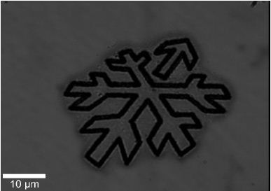
Figure 1. White light image of the lithographically written structure in Si.
Confocal PL Imaging
The same laser used for Raman imaging was also used for confocal PL imaging. In this case, a specially selected 50X NA 0.8 objective was used that enabled the best throughput for the PL signal (in the range of 1000-1250nm for Si) while demonstrating minimal chromatic aberration between the PL peak and the excitation wavelength (532nm).
The signal was collected using a 100µm core diameter multi-mode fiber and the same was delivered to a SpectraPro 2300i mirror based spectrometer using an InGaAs CCD camera 1024 pixels in width and a 150g/m grating. Then, a scan of 50x100µm2 with 100x100 points and 0.210s integration time per spectrum was carried out.
Atomic Force Microscopy
The measurements were done in AC mode using a force modulation cantilever with a resonance frequency of 87kHz. The first overview scan was done on an area of 50x50µm with 512x512 points. A second scan was done on an area of 14x14µm2 and 256x256 points.
Results and Discussion
At the specified laser power, it took approximately 2 minutes for writing the structure. After this, it was possible to view the white light image as shown in Figure 1. The image was then recorded with the WITec Control software using the integrated video camera.
Once the planar confocal Raman image scan was performed, it was possible to obtain the image shown in Figure 2a from the integrated intensity of the first order Si band near 520 rel.i/cm. Figure 2b depicts the intensity profile along the blue cross-section displayed in Figure 2a.
An increased intensity of the Si signal close to the laser scribed structure as well as a strong decrease exactly along it was seen in both the image and the cross-section. The cross section shows a FWHM of the intensity profile of 680nm. As the system is diffraction-limited, the laser for scribing the structures was as narrow as 355nm full width half maximum (FHWM).
While the same structures were scanned again with a diffraction-limited resolution, the Gaussian profile of the laser during the Raman measurement is convoluted with the geometry of the structure itself. In order to check this, a depth scan was conducted along the line marked in green in Figure 2a. The result is clearly shown in Figure 3a where the integrated intensity of the 1st order Si peak is illustrated.
The observations also revealed that the intensity originates from approximately the same height and that a very small signal originates from the positions where the laser-scribed structures are located. It can also be noted that brighter areas are located right next to the structures. Figure 3b shows the intensity profile obtained along the turquoise line.
![Confocal Raman Image of the intensity of the first order Si line [a] and the intensity profile along the cross section marked in blue [b]. The green line in [a] indicates where the depth scan was performed.](https://www.azonano.com/images/Article_Images/ImageForArticle_3769_44895971474155096368.jpg)
![Confocal Raman Image of the intensity of the first order Si line [a] and the intensity profile along the cross section marked in blue [b]. The green line in [a] indicates where the depth scan was performed.](https://www.azonano.com/images/Article_Images/ImageForArticle_3769_44895971475486113168.jpg)
Figure 2. Confocal Raman Image of the intensity of the first order Si line [a] and the intensity profile along the cross section marked in blue [b]. The green line in [a] indicates where the depth scan was performed.
![Confocal Raman Image of the intensity of the first order Si line along a depth scan [a] and the intensity profile along the cross section marked in turquoise [b].](https://www.azonano.com/images/Article_Images/ImageForArticle_3769_44895971476793987423.jpg)
![Confocal Raman Image of the intensity of the first order Si line along a depth scan [a] and the intensity profile along the cross section marked in turquoise [b].](https://www.azonano.com/images/Article_Images/ImageForArticle_3769_448959714779629657177.jpg)
Figure 3. Confocal Raman Image of the intensity of the first order Si line along a depth scan [a] and the intensity profile along the cross section marked in turquoise [b].
For the study, the sophisticated fitting option in the WITec Project Plus software was utilized and a Lorenzian curve was fitted to the spectra. It can be seen from the results that the exact peak position is obtained and is plotted for the planar scan in Figure 4a and for the depth scan in Figure 4c. Figure 4b displays two averaged, representative spectra with the corresponding fitted Lorenzian curves.
To further examine the laser-scribed structures, a confocal PL scan was also conducted. Figure 5a illustrates the integrated intensity of the Si PL signal and Figure 5b shows the PL spectrum itself. This spectrum was obtained with 210ms integration time right in the center of the structure and only the camera background signal was subtracted (no smoothing or averaging was applied).
![Confocal Raman Image of the position of the first order Si line in the planar scan [a] and in the depth scan [c]. Two representative spectra showing the shift are shown.](https://www.azonano.com/images/Article_Images/ImageForArticle_3769_4489597147910882483.jpg)
![Confocal Raman Image of the position of the first order Si line in the planar scan [a] and in the depth scan [c]. Two representative spectra showing the shift are shown.](https://www.azonano.com/images/Article_Images/ImageForArticle_3769_44895971480428246046.jpg)
![Confocal Raman Image of the position of the first order Si line in the planar scan [a] and in the depth scan [c]. Two representative spectra showing the shift are shown.](https://www.azonano.com/images/Article_Images/ImageForArticle_3769_44895971481689814094.jpg)
Figure 4. Confocal Raman Image of the position of the first order Si line in the planar scan [a] and in the depth scan [c]. Two representative spectra showing the shift are shown.
![Confocal PL Image of the intensity of the PL signal of Si in a planar scan [a] and a representative PL spectrum which originates from the center of the structure [b].](https://www.azonano.com/images/Article_Images/ImageForArticle_3769_4489597148281256055.jpg)
![Confocal PL Image of the intensity of the PL signal of Si in a planar scan [a] and a representative PL spectrum which originates from the center of the structure [b].](https://www.azonano.com/images/Article_Images/ImageForArticle_3769_44895971484189821813.jpg)
Figure 5. Confocal PL Image of the intensity of the PL signal of Si in a planar scan [a] and a representative PL spectrum which originates from the center of the structure [b].
The Raman and the PL scans demonstrates that at areas where the laser-scribing took place, the structures emitted a weaker Raman and PL signal. An AFM overview scan is shown in Figure 6a and a zoomed-in scan focusing on one of the arrows is shown in Figure 6b.
It can be seen from both the AFM images that there is a higher topography along the structure and from figure 6b it can clearly be seen that dot-like structures are present along the written structure. The AFM images show that significant structural changes took place in the Si where the laser scribing took place.
![AFM Scan of the structure. Overview[a] and zoomed scan onto one of the structures[b].](https://www.azonano.com/images/Article_Images/ImageForArticle_3769_448959714857523145021.jpg)
Figure 6. AFM Scan of the structure. Overview[a] and zoomed scan onto one of the structures[b].
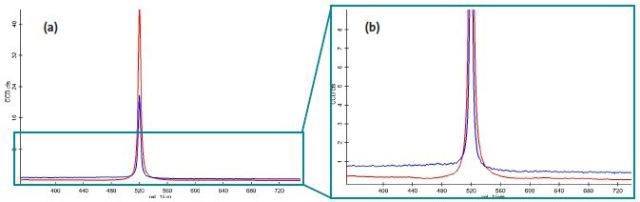
Figure 7. Raman Spectra well outside the structure (red) and inside the grooves (blue)
The spectra show a strong increase in the 1st order Si peak intensity and an increase in the signal background. It must be noted that the background is more on the low wave number side of the Si peak in comparison with the high wave number side of it.
Conclusion
This article shows how confocal Raman imaging, confocal PL imaging, laser-scribing and AFM in a single microscopy system was performed on a crystalline Si sample. The same electronics and software i.e. alphaControl and WITecControl were used to control all the experiments. It was possible to clearly detect the written structures with all the measurement techniques.
The Raman and the PL signal originating from crystalline Si are considerably reduced at the laser-scribed structures and one can detect abroad enhancement of the signal background of the Raman Si signal. By using AFM measurements, it was possible to exclude narrow grooves, which were the cause for the reduced Raman and PL signal, and demonstrated that the structures included dot-like elevations.

This information has been sourced, reviewed and adapted from materials provided by WITec GmbH.
For more information on this source, please visit WITec GmbH.