This article has been updated in January 2024.
High resolution images of microscopic samples can be obtained experimentally using Scanning Electron Transmission Microscopy (STEM). It is an effective method for examining the intricate structure of nanomaterials used in developing nanotechnology.

Image Credit: Jeff Whyte/Shutterstock.com
For nanoscience applications, electron microscopy has become one of the key characterization methods. This is because, in comparison to standard optical microscopy methods, electron microscopies can achieve much greater spatial resolutions.
As light travels through a slit, it is diffracted and the light waves spread out (Figure 1). The waves will constructively or destructively interfere with each other, resulting in the formation of bright and dark lines on a screen.
The wavelength of the light determines the amount of diffraction the wave undergoes. Red light exhibits the most diffraction in the visible light spectrum because of its longer wavelength. Light with longer wavelengths diffracts more than light with shorter wavelengths. As can be seen in Figures 2(a) and 2(b), images created with red light are consequently blurrier than those created with UV or blue light. These phenomena is what gives rise to the Abbe diffraction limit for a microscope – ultimately determining the smallest objects that can be resolved.
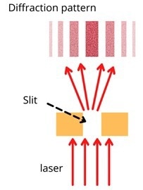
Figure 1. Illustration of light diffraction. Image Credit: Ilamaran Sivarajah
As can be seen in Figures 2(a) and 2(b), images created with red light are consequently blurrier than those created with UV or blue light. These phenomena is what gives rise to the Abbe diffraction limit for a microscope – ultimately determining the smallest objects that can be resolved.
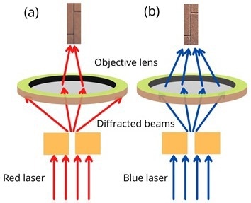
Figure 2. Illustration of an image of an object formed after the diffracted light beams from (a) a red laser and (b) a blue laser are focused using a lens. Image Credit: Ilamaran Sivarajah
Development of Electron Microscopy
The first electron microscopes were developed in 1933, making it possible to build much higher-resolution microscopes.
The two main kinds of electron microscopy are transmission electron microscopes (TEMs) and scanning electron microscopes (SEMs). Scanning transmission electron microscopy (STEM) combines the spatial scanning capabilities of SEM with the detection geometries used in TEM to provide information that can be used for detailed local chemical analysis and spatial reconstruction of the object.
Figure 3(a) depicts the fundamental operating principle of a TEM. An electron gun generates an electron beam source. A condenser lens, an objective lens, and a projector lens are all parts of the TEM and from the lens stack used to shape and control the electron beam (Figure 3(a)).
In TEM, the sample is measured in a transmission geometry where the beam is passed directly through the sample on a camera placed behind. In SEM, rather than just using a wide beam to measure the entire sample at once, the beam is rastered over the sample by moving the focused electron using the scanning coil. In SEM, detection and image reconstruction are normally performed by collection of the backscattered electrons, which can also be used to provide elemental composition information.
Impact of STEM in Nanotechnology
The same scanning principle as SEM is used in STEM, but the images are acquired in a transmission geometry. There is no need for a projector or objective lens in a STEM image as the beam is scanned over the sample, which also makes it possible to include additional auxiliary detectors to provide more analytical information on the sample.
Nanoscale spatial resolution has made STEM invaluable for nanotechnology applications and many STEM measurements also make use of additional devices for sample manipulation to make measurements closer to in operando conditions.
Some general examples of the types of measurements and characterizations performed with STEM include studying the sizes, shapes, defects, surface structures and electronic states of nanoparticle systems.
Some examples of STEM imaging applications include studying environmental effects on copper nanoparticles. The ability to include additional equipment in STEM, such as heating samples to very high temperatures and flowing gas over a sample, makes it possible to do in situ environmental studies.
In this case, the oxidation process could be monitored and the movement of the copper cations from the inner and outer regions could be seen, as well as any electron beam-induced oxidation that was not driven by the increase in temperature or the addition of gas.
Another very active area of nanoscience research with STEM is the study of interfaces. Interfaces are unusual in that their properties are often very different from those of the bulk material, but they can be challenging to study due to their limited size.
STEM can be used to look at interactions between the substrate and surface at interfacial regions and even to measure the mechanical or interactive forces between the species.
Many interfacial studies in STEM make use of liquid cells where a solid surface and be mixed with a contained liquid.
Key application areas for this include corrosion or process studies, where the high spatial resolution of STEM has made it possible to see how gas bubbles are formed during working processes like electrochemical water splitting for clean hydrogen generation.
The operando characterization of liquid/solid electrolytes is also popular in battery research, where STEM is used to study the delithiation processes that ultimately can destroy the electrodes and limit battery lifetimes.
More advanced variations of STEM are proving invaluable for battery studies in particular, such as 4D versions of the technique that can provide not just 3D spatial information on the sample but can monitor the temporal response of the sample, often over timescales shorter than picoseconds. 4D STEM has also been applied to watch the delithiation processes in batteries as they occur and a number of other electrochemical processes.
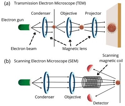
Figure 3. Schematic diagrams of (a) Transmission Electron Microscope (TEM) and (b) Scanning Electron Microscope (SEM). Image Credit: Ilamaran Sivarajah
Many quantitative techniques for evaluating interactive forces or mechanical properties of nanomaterials based on STEM have been developed, meaning the tool can not just be used for imaging structures or working out elemental compositions but for evaluating the behavior of a nanoobject.
With attempts to develop nanomachinery that perform mechanical work becoming more common with advances in fabrication techniques, STEM is becoming an ever more invaluable analysis and characterization tool.
References and Further Reading
Liu J. (2005) Scanning transmission electron microscopy and its application to the study of nanoparticles and nanoparticle systems. J Electron Microsc (Tokyo). Jun;54(3):251-78. https://doi.org/10.1093/jmicro/dfi034
Brodusch N, Demers H, Gauvin R. (2018) Imaging with a Commercial Electron Backscatter Diffraction (EBSD) Camera in a Scanning Electron Microscope: A Review. Journal of Imaging. 4(7):88. https://doi.org/10.3390/jimaging4070088
Golding, C., Lamboo, L., Beniac, D. et al. (2016) The scanning electron microscope in microbiology and diagnosis of infectious disease. Sci Rep 6, 26516 https://doi.org/10.1038/srep26516
Serra-maia, R., Kumar, P., Meng, A. C., Foucher, A. C., Kang, Y., Karki, K., Jariwala, D., & Stach, E. A. (2021). Nanoscale Chemical and Structural Analysis during In Situ Scanning/Transmission Electron Microscopy in Liquids. ACS Nano, 15, 10228–10240. https://doi.org/10.1021/acsnano.1c02340
Shorokhov, D., & Zewail, A. H. (2008). 4D electron imaging: principles and perspectives. Phys Chem Chem Phys, 10(20), 2879–2893. https://doi.org/10.1039/b801626g
Disclaimer: The views expressed here are those of the author expressed in their private capacity and do not necessarily represent the views of AZoM.com Limited T/A AZoNetwork the owner and operator of this website. This disclaimer forms part of the Terms and conditions of use of this website.