Transmission Electron Microscopy, or TEM, lets scientists see the invisible. Opening a window into the nanoscale, TEM reveals structural topography with precision, exposing everything from smooth planes to unwanted defects.1
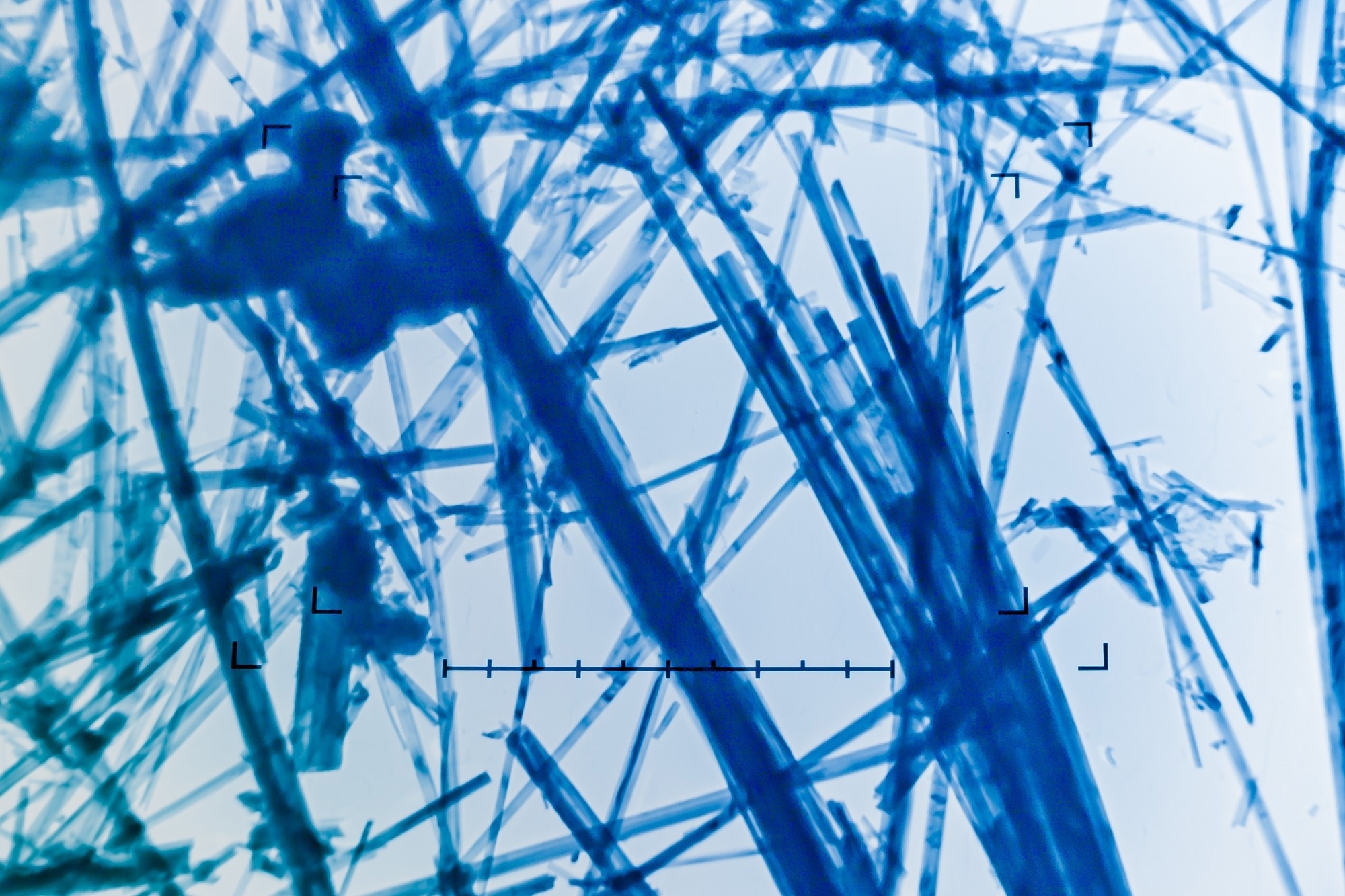 Image Credit: Pvince73/Shutterstock.com
TEM is an advanced characterization tool that uses a focused beam of electrons to reveal the smallest details on material surfaces. TEM can image individual atoms, lattice arrangements, and structural defects. It's an indispensable tool for advancing material design and supporting nanotechnology research.1
Principles of TEM
TEM works by accelerating electrons, typically with energies between 80 and 300 kV, and directing them through a specimen thin enough for electron transmission. Because of their very short wavelength (around 0.0025 nm at 200 kV), electrons can resolve structures at the sub-nanometer level, far beyond the resolution limits of light microscopy.2
As electrons pass through a sample, they interact with its structure, producing scattered signals. These are converted into images or diffraction patterns using electromagnetic lenses and detectors. Elastic scattering produces contrast in bright-field or dark-field imaging modes, while inelastic scattering enables spectroscopic analysis.2
Most modern TEMs are equipped with high-resolution TEM (HRTEM), scanning TEM (STEM), and other analytical extensions. HRTEM resolves atomic lattice fringes, while selected area electron diffraction (SAED) captures crystallographic information from defined regions. STEM, which scans a focused probe across the sample, offers atomic-number contrast (Z contrast) and is often paired with energy-dispersive X-ray spectroscopy (EDS) or electron energy-loss spectroscopy (EELS) for chemical analysis.2
TEM Imaging at the Nanoscale
TEM is particularly effective at characterizing individual nanostructures, something bulk techniques like X-ray diffraction (XRD) cannot do. Its spatial resolution and imaging versatility make it incredibly useful in heterogeneous or low-dimensional materials where statistical averages may obscure important features.
Morphology and Particle Size
TEM enables direct observation of nanoparticle morphology, shape uniformity, and size distribution. In a study in RSC Advances on ZnO nanowires and nanosheets, for instance, TEM revealed prismatic and plate-like forms with aspect ratios that were difficult to capture with XRD. Statistical analysis of TEM images revealed particle dimensions with nanometer precision.3
Similarly, a paper on gold nanoparticles explored aberration-corrected TEM and STEM analyses. It demonstrated differences in lattice fringe quality and contrast, allowing researchers to study their crystalline domains more accurately than would have been possible with conventional microscopy.4
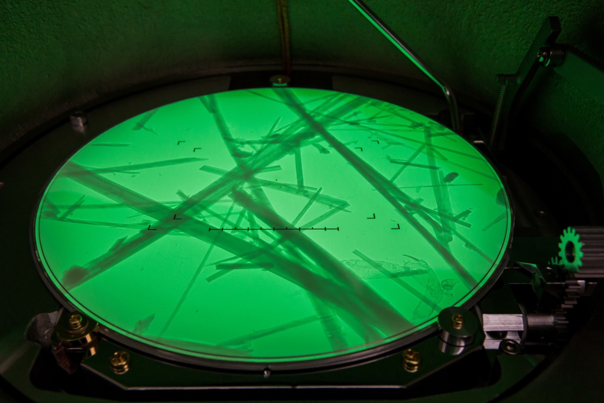 Image Credit: Pvince73/Shutterstock.com
Crystal Structure and Defects
HRTEM is able to resolve interplanar spacings and lattice orientations. In a paper by Panda et al., this method was used to characterize the structure of ZnO nanowires, with lattice spacings of 0.281 nm and 0.260 nm corresponding to (010) and (002) planes resolved, confirming growth along the [001] direction.3
SAED and lattice imaging confirmed this structure. SAED patterns help to distinguish between single-crystal and polycrystalline domains, and can quantify orientation distributions. TEM also reveals structural defects, such as dislocations or stacking faults, that play a critical role in properties like conductivity and catalytic activity. SAED further confirmed the structure through concentric diffraction rings, which indicate a polycrystalline nature, and provided quantitative data on crystallinity and aspect ratios.3
Aberration-corrected STEM was instrumental in visualizing single-atom catalysts on oxide supports. These atomic-scale images are able to improve understanding of active site configurations and their chemical environments.5
Chemical and Elemental Information
When combined with EELS or EDS, TEM enables nanoscale elemental mapping of a surface. This has been applied to a range of materials, such as Fe-Co nanoparticles embedded in carbon matrices, where the technique helped to verify alloy composition and dispersion.6
In a more biological context, EDS has helped identify metallic and oxide nanoparticles within tissues, providing both spatial and compositional data. These spectroscopic capabilities allow researchers to correlate structure with local chemistry, which is essential for tailoring functional materials.
Basics of TEM Sample Preparation
Successful TEM analysis depends on careful sample preparation. Most specimens must be thinner than 100 nm. Nanoparticles are typically drop-cast onto carbon-coated grids, while nanowires or nanosheets may require embedding and microtoming. Thin films are prepared using focused ion beam (FIB) milling. Biological samples require fixation, embedding, and ultrathin sectioning, or cryo-TEM, to preserve hydration and minimize artefacts.
Transmission Electron Microscope (TEM) | How do Electron Microscopes Work?
Video Credit: MEDICAL TECHNOLOGY/YouTube.com
Preparation is often the most time-intensive part of the process, and if not done correctly, it can introduce distortions. Electron beam exposure can also damage sensitive materials, in particular soft matter and very small nanoparticles.
Where TEM Makes a Difference
TEM is widely used across fields where nanostructure dictates function. Metallic nanoparticles such as Au, Ag, and Pt are routinely imaged at atomic resolution. In nanomedicine, researchers have used TEM to track gold nanoparticles within cells, identifying their location in the cytosol, endosomes, and nuclei.7
Cross-sectional TEM is essential in thin-film analysis, resolving grain size, layer interfaces, and defects in semiconductor and oxide materials. Such analysis is important in semiconductor nanostructures and oxide thin films.
Papavasiliou et al. reported that TEM tomography of Pt-loaded CeO2 nanocomposites revealed the three-dimensional distribution of platinum nanoparticles on ceria supports, providing valuable insights into catalyst design. Similarly, TEM has been applied to evaluate the distribution of polymeric or lipid nanoparticles in biological systems.8
Interested in other EM techniques? Read about SEM here!
Limitations of TEM
While TEM provides unparalleled spatial resolution, it has limitations. Only thin sections can be analyzed, which often are not representative of the bulk material. Beam sensitivity is a concern for organic or polymer-based samples. TEM is also static, offering snapshots rather than dynamic behavior, although in situ TEM addresses this constraint.9
Additionally, the technique requires significant financial investment and expertise - TEM instruments are costly to purchase and maintain, and their operation demands highly skilled personnel.
Finally, while TEM excels in providing localized, high-resolution information, it lacks the statistical averaging capability of bulk characterization methods such as XRD or other ensemble techniques, which can better represent the overall properties of a material.1, 9
Advancements in TEM for Nanomaterial Research
Recent advances have extended TEM's capabilities. Aberration correction now allows imaging below one angstrom, revealing atomic arrangements and defects with precision.
Electron tomography has introduced three-dimensional reconstruction techniques that reveal the spatial arrangement of nanoparticles and nanocomposites in unprecedented detail. Cryo-TEM enables the observation of biological and soft nanostructures in their native, hydrated state without introducing artifacts from drying or staining.8
Correlative states, combining TEM with fluorescence microscopy or atomic force microscopy for example, are bridging length scales and linking structure with function.9
Conclusion
Transmission Electron Microscopy has quietly become indispensable in the structural analysis of nanomaterials. Its ability to combine imaging, diffraction, and spectroscopy enables a comprehensive understanding of morphology, particle size, crystallinity, and composition at the nanoscale.
Looking ahead, integrating TEM with complementary techniques such as XRD, SEM, and in situ analyses will offer a more comprehensive understanding of nanomaterials. This integrated approach will enhance the precision of structural characterization and drive the rational design and innovative application of nanomaterials across a wide range of scientific and technological disciplines.
References and Further Studies
- Anjum, D. H. In Characterization of Nanomaterials with Transmission Electron Microscopy, IOP Conference Series: Materials Science and Engineering, IOP Publishing: 2016; p 012001.
- Mast, J.; Verleysen, E.; Hodoroaba, V.-D.; Kaegi, R., Characterization of Nanomaterials by Transmission Electron Microscopy: Measurement Procedures. Characterization of Nanoparticles, Elsevier: 2020; pp 29-48.
- Panda, S. A.; Choudhary, S.; Barala, S.; Hazra, A.; Jena, S. K.; Gangopadhyay, S., Surface Energy and Stress Driven Growth of Extremely Long and High-Density Zno Nanowires Using a Thermal Step-Oxidation Process. RSC advances 2024, 14, 28086-28097.
- Mayoral, A.; Deepak, F. L.; Esparza, R.; Casillas, G.; Magen, C.; Perez-Tijerina, E.; Jose-Yacaman, M., On the Structure of Bimetallic Noble Metal Nanoparticles as Revealed by Aberration Corrected Scanning Transmission Electron Microscopy (Stem). Micron 2012, 43, 557-564.
- Tieu, P.; Yan, X.; Xu, M.; Christopher, P.; Pan, X., Directly Probing the Local Coordination, Charge State, and Stability of Single Atom Catalysts by Advanced Electron Microscopy: A Review. Small 2021, 17, 2006482.
- Falqui, A.; Corrias, A.; Gass, M.; Mountjoy, G., A Transmission Electron Microscopy Study of Fe-Co Alloy Nanoparticles in Silica Aerogel Matrix Using Hrem, Edx, and Eels. Microscopy and Microanalysis 2009, 15, 114-124.
- Drescher, D.; Bu¨chner, T.; Schrade, P.; Traub, H.; Werner, S.; Guttmann, P.; Bachmann, S.; Kneipp, J., Influence of Nuclear Localization Sequences on the Intracellular Fate of Gold Nanoparticles. ACS nano 2021, 15, 14838-14849.
- Papavasiliou, J.; Paxinou, A.; Slowik, G.; Neophytides, S.; Avgouropoulos, G., Steam Reforming of Methanol over Nanostructured Pt/Tio2 and Pt/Ceo2 Catalysts for Fuel Cell Applications. Catalysts 2018, 8, 544.
- Malatesta, M., Transmission Electron Microscopy as a Powerful Tool to Investigate the Interaction of Nanoparticles with Subcellular Structures. International journal of molecular sciences 2021, 22, 12789.
Disclaimer: The views expressed here are those of the author expressed in their private capacity and do not necessarily represent the views of AZoM.com Limited T/A AZoNetwork the owner and operator of this website. This disclaimer forms part of the Terms and conditions of use of this website.