The characterization of nanomaterials demands analytical tools capable of resolving structures far below the limits of optical microscopy. Scanning Electron Microscopy (SEM) has emerged as one of the most widely used techniques for structural analysis at the nanoscale.1
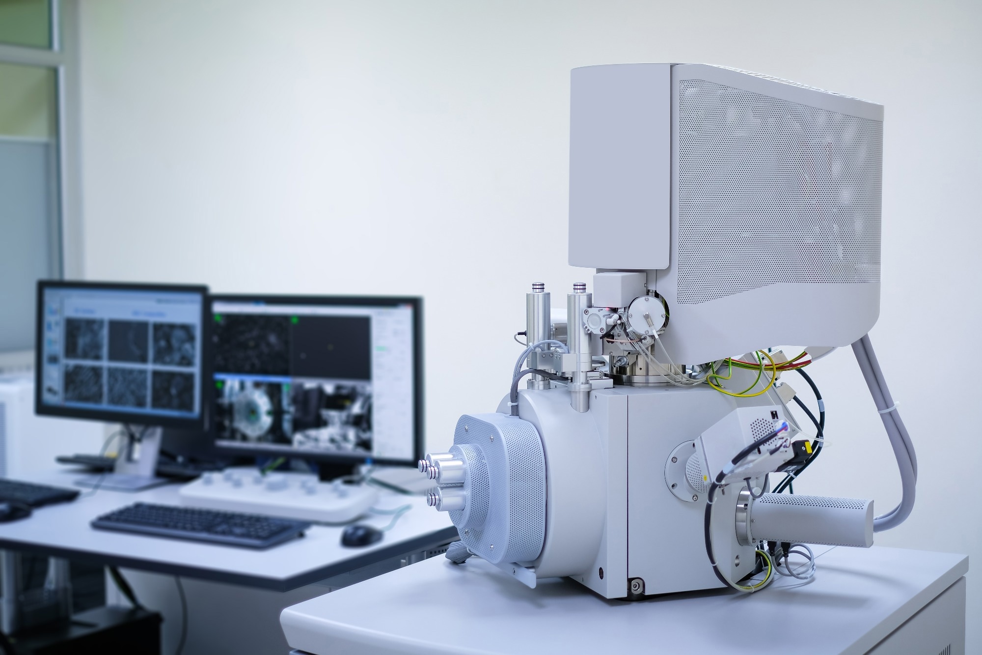
Image credit: Anucha Cheechang/Shutterstock.com
Unlike optical microscopy, SEM does not rely on light waves but instead uses a beam of electrons to interact with materials, enabling magnifications up to 300,000× and resolutions approaching 1 nm.1
With its ability to generate high-resolution, three-dimensional images of surfaces, SEM provides critical insights into morphology, particle size, surface topography, and even crystallinity. These capabilities make SEM a central tool in studying nanoparticles, nanowires, thin films, and porous frameworks, where structural features often dictate material functionality.1-2
Principles of SEM
The SEM system consists of an electron column containing the electron gun, electromagnetic lenses, scanning coils, and a detector system housed within a vacuum chamber.3
SEM operates by directing a focused electron beam scanned in a raster pattern across a specimen's surface. When these high-energy electrons interact with atoms in the sample, they generate various signals, such as secondary electrons (SEs), backscattered electrons (BSEs), and characteristic X-rays, which are detected and converted into images or spectra.3
- Secondary electrons (SEs): Low-energy electrons (<50 eV) emitted from atoms near the surface. Because of their shallow escape depth (typically <10 nm), they provide fine detail about surface topography.
- Backscattered electrons (BSEs): Higher-energy electrons (>50 eV) elastically scattered by atomic nuclei. Their intensity depends strongly on atomic number, making them useful for compositional contrast.
- Characteristic X-rays: Emitted when inner-shell vacancies created by the electron beam are filled. Energy-dispersive X-ray spectroscopy (EDS/EDX) enables elemental analysis alongside imaging.3
Two main types of electron sources are commonly employed. The first are thermionic emitters, usually tungsten filaments, which emit electrons when heated. These are robust and cost-effective, though they provide relatively low brightness. The second type is field emission guns, which exploit quantum tunneling at a sharp tip under a strong electric field.3
Field emission guns deliver high brightness and produce very small spot sizes, enabling imaging with sub-nanometer resolution. Recent advances, including improved detector geometries, quantitative signal calibration, and optimized low-voltage operation, have enhanced SEM by making it possible to analyze delicate or insulating nanomaterials without damaging them.3
Imaging Capabilities at the Nanoscale
SEM provides several advantages for nanoscale imaging. Modern field emission SEMs achieve lateral resolutions near one nanometer, and their large depth of field allows three-dimensional visualization of complex surfaces, which is particularly valuable for examining rough or hierarchical nanostructures.4
SEM can emphasize surface morphology or compositional contrast by selecting secondary or backscattered electron signals. Unlike transmission electron microscopy, SEM does not require ultrathin sections, so bulk specimens, thin films, or powders can often be imaged with minimal preparation.4
Furthermore, environmental SEM enables imaging of hydrated or beam-sensitive samples under low vacuum or atmospheric conditions, while low-voltage operation reduces charging and beam damage, allowing the study of organic or polymeric nanomaterials.4
Structural Information Revealed by SEM
Morphology and Particle Size
SEM excels at determining nanoparticle size, shape, and distribution. For example, metallic nanoparticles (Au, Ag, Pt) and oxide particles (TiO2, ZnO) are readily imaged to confirm uniformity and degree of agglomeration. Nanowires and nanotubes can be analyzed for diameter, length, and alignment, providing insight into growth mechanisms and functional properties.1,3
In addition to qualitative assessment, digital image analysis software is frequently used to generate particle size distributions from SEM micrographs, providing statistically meaningful measurements that complement visual aspects.5
Surface Features
The high surface sensitivity of scanning electron imaging makes SEM invaluable for analyzing porosity, roughness, and surface steps. High-resolution SEM has even resolved terraces as small as 1.2 nm on zeolite crystals, highlighting its capability to probe superfine surface structures.3
Crystallinity and Orientation
While transmission electron microscopy (TEM) remains the primary tool for atomic-scale crystallography, SEM contributes through electron channeling contrast imaging (ECCI) and orientation contrast BSE imaging. These methods reveal grain orientation, defects, and domain structures in polycrystalline thin films and nanostructured materials.3
Composition and Phase Distribution
BSE imaging provides strong contrast between regions of different atomic number, enabling visualization of multiphase composites, core–shell nanostructures, and embedded inclusions. Coupled with EDX analysis, SEM can map elemental distributions across heterogeneous nanomaterials.3
Examples of Nanomaterials Studied with SEM
SEM has been widely applied to various nanomaterials, each with distinct structural features that can be directly observed. In the case of gold nanoparticles studied by Silva et al., used in biomedical imaging and catalysis, SEM reveals particle size uniformity and surface coatings, which are critical for reproducibility, while TiO2 nanoparticles studied for photocatalysis by Dantas et al. can be examined for agglomeration and surface roughness that influence activity.6,7
SEM provides rapid visualization of nanowires and nanotubes, including carbon nanotubes and semiconductor nanowires, their aspect ratios and degree of alignment, parameters essential for electronic and photonic device fabrication.8
Thin films used in photovoltaics and electronics also benefit from SEM analysis, as imaging can reveal thickness, uniformity, and defects such as cracks or pinholes; in oxide and perovskite films, surface morphology observed by SEM often correlates directly with device efficiency.9
SEM particularly well serves porous frameworks such as zeolites, mesoporous silica, and metal-organic frameworks because overlapping diffraction peaks complicate X-ray characterization. SEM can directly visualize pore openings and hierarchical structures, confirming connectivity and accessibility.10
Core-shell and composite nanostructures, such as yolk shell Au@TiO2 systems, have also been imaged to show internal voids and shell integrity, insights critical for catalysts and controlled drug delivery applications.11
Sample Preparation and Challenges
Despite its versatility, SEM requires careful sample preparation to obtain meaningful results. Nonconductive samples such as oxides, polymers, and biological nanomaterials tend to accumulate charge under the electron beam, which leads to image distortion.2,3
To address this, specimens are often sputter-coated with thin conductive layers of gold, platinum, or carbon. However, low-voltage imaging and environmental SEM can sometimes reduce or eliminate the need for coating. Traditional SEM also requires high vacuum conditions, so volatile or hydrated samples must be dried or imaged using environmental SEM.3
In addition, high-energy electron beams can cause heating, bond breaking, or structural changes in delicate nanomaterials such as metal-organic frameworks, perovskites, or organic-inorganic hybrids, making it necessary to optimize accelerating voltage and beam current to minimize damage.3
Finally, SEM is inherently surface-sensitive and primarily probes near-surface regions, so transmission electron microscopy is more appropriate for examining internal crystallography or atomic-scale defects.3
Recent Advances in SEM for Nanomaterials
Recent technological progress has further enhanced the role of SEM in nanomaterials research. The lens detectors now enable the collection of electrons at low landing energies, improving resolution and reducing charging effects in insulating materials.1
Recently, Li et al. reported that atmospheric SEM makes it possible to perform in situ imaging in liquid or gaseous environments. It is particularly valuable for studying dynamic processes such as electrochemical reactions or biological interfaces. Developments in aberration correction and improved electron sources are expected to provide even higher spatial resolution and greater stability in future instruments.12
In addition, correlative microscopy, which combines SEM with techniques such as TEM, atomic force microscopy, or spectroscopy, is increasingly applied to gain a more holistic understanding of nanomaterial structure and function.3
References and Further Studies
- Akhtar, K.; Khan, S. A.; Khan, S. B.; Asiri, A. M., Scanning Electron Microscopy: Principle and Applications in Nanomaterials Characterization. In Handbook of Materials Characterization, Springer: 2018; pp 113-145.
- Prasad, R. D.; Prasad, R. S.; Prasad, R. B.; Prasad, S. R.; Singha, S. B.; Singha, D.; Prasad, R. J.; Sinha, P.; Saxena, S.; Vaidya, A. K., A Review on Modern Characterization Techniques for Analysis of Nanomaterials and Biomaterials. ES Energy & Environment 2024, 23, 1087.
- Suga, M.; Asahina, S.; Sakuda, Y.; Kazumori, H.; Nishiyama, H.; Nokuo, T.; Alfredsson, V.; Kjellman, T.; Stevens, S. M.; Cho, H. S., Recent Progress in Scanning Electron Microscopy for the Characterization of Fine Structural Details of Nano Materials. Progress in Solid State Chemistry 2014, 42, 1-21.
- Akhtar, S.; Ali, S., Characterization of Nanomaterials: Techniques and Tools. In Applications of Nanomaterials in Human Health, Springer: 2020; pp 23-43.
- Liang, C.; Jia, Z.; Chen, R., An Automated Particle Size Analysis Method for SEM Images of Powder Coating Particles. Coatings 2023, 13(9), 1547.
- Dantas, S. R. A.; de Oliveira Romano, R. C.; Vittorino, F.; Loh, K., Effects of Surface Roughness and Light Scattering on the Activation of TiO2 on Mortar Photocatalytic Process. Construction and Building Materials 2021, 270, 121421.
- Silva, S. M.; Tavallaie, R.; Sandiford, L.; Tilley, R. D.; Gooding, J. J., Gold Coated Magnetic Nanoparticles: From Preparation to Surface Modification for Analytical and Biomedical Applications. Chemical Communications 2016, 52, 7528-7540.
- Kolahdouz, M.; Xu, B.; Nasiri, A. F.; Fathollahzadeh, M.; Manian, M.; Aghababa, H.; Wu, Y.; Radamson, H. H., Carbon-Related Materials: Graphene and Carbon Nanotubes in Semiconductor Applications and Design. Micromachines 2022, 13, 1257.
- Panjan, P.; Drnovšek, A.; Gselman, P.; Cekada, M.; Panjan, M., Review of Growth Defects in Thin Films Prepared by PVD Techniques. Coatings 2020, 10, 447.
- Liang, J.; Liang, Z.; Zou, R.; Zhao, Y., Heterogeneous Catalysis in Zeolites, Mesoporous Silica, and Metal–Organic Frameworks. Advanced Materials 2017, 29, 1701139.
- Chen, Y.-A.; Wang, Y.-T.; Moon, H. S.; Yong, K.; Hsu, Y.-J., Yolk–Shell Nanostructures: Synthesis, Photocatalysis and Interfacial Charge Dynamics. RSC Advances 2021, 11, 12288-12305.
- Li, Y.; Ning, Q.; Xu, H.; Li, S.; Wang, J.; Wang, L.; Chen, S.; Zhang, S.; Wang, J.; Hu, Z., Imaging Gas-Involved Structural Dynamics by Environmental Electron Microscopy. Small 2025, 21, 2411415.
- Gupta, P.; Rai, N.; Verma, A.; Gautam, V., Microscopy Based Methods for Characterization, Drug Delivery, and Understanding the Dynamics of Nanoparticles. Medicinal Research Reviews 2024, 44, 138-168.
Disclaimer: The views expressed here are those of the author expressed in their private capacity and do not necessarily represent the views of AZoM.com Limited T/A AZoNetwork the owner and operator of this website. This disclaimer forms part of the Terms and conditions of use of this website.