Experiments conducted by a group of scientists from the Materials Sciences Division at the Lawrence Berkeley Lab and the University of California have shown that graphene on boron nitride (BN) retains the intrinsic properties of graphene more than on any other substrate.
The research team was led by Michael Crommie and Alex Zettl. The research findings were published in Nano Letters. Regis Decker, the lead author of the article, noted that the best way to study the intrinsic properties of graphene is to conduct the experiment on suspended graphene. But when investigated with STM (scanning tunnelling microscopy), suspended graphene is quite unstable so it becomes essential to find a substrate that is identical to suspended graphene.
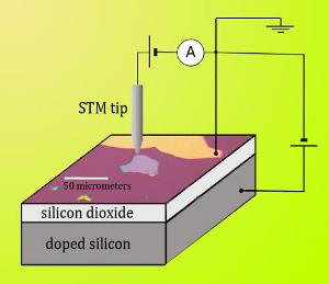 The researchers deposited boron nitride flakes on a layer of silicon dioxide, grown on a layer of doped silicon. The doped silicon was used as a gate electrode for doping the graphene during scanning tunneling microscopy. Graphene was applied to both the boron nitride flakes (under the STM tip) and the bare silicon dioxide; the graphene (dark and light purple) was grounded by an electrode of gold/titanium (gold). The STM could scan across both substrate systems.
According to Decker, BN has a large electronic band gap with the absence of dangling bonds and is extremely flat, hence it is a suitable substrate for graphene. BN has a hexagonal structure (h-BN) with boron and nitrogen items arranged alternately which is very similar to the way carbon atoms are arranged in graphene.
Considering the size, the h-BN lattice is 1.7% more than that of graphene yet they can be aligned on top of one another in a closer manner than any other substrate. In order to create graphene/BN devices, strips of Scotch Tape were used to exfoliate BN crystals into minute flakes. These flakes were then deposited on a silicon dioxide layer which was formed on a doped silicon layer. The doped silicon layer is utilized as a gate electrode to monitor the charge concentration and enables doping of the graphene layer above during STM.
After placing the graphene sheets obtained by chemical vapour deposition on copper on the BN flakes, the assembly was then annealed at high temperatures. A titanium gold electrode was deposited on graphene to ground the graphene layer and the silicon layer acts as the gate electrode. A total of three graphene/BN devices were created for making STM comparisons with graphene on silicon dioxide. The STM tip was made to scan the graphene layer, determining topography and concentrations of local charges at different doping levels determined by the silicon layer gate electrode.
Topographically, graphene on BN is not as rough as graphene on silicon, with the variations in height on the scanned surface, being only around 40 pm. Differences in charge density were much lesser in the BN substrate and fewer impurities were found.