An easy-to-implement method for stamping very minute patterns onto special type of nanomaterials has been established which could be used in solar cells and devices used for delivery of drugs.
The method was established by engineers from the Vanderbilt University. It was explained in detail in the May issue of the Nano Letters journal. The method can function with nanomaterials that feature minute voids to render distinct electrical, optical, mechanical and chemical properties.
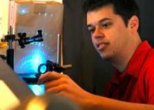 Diffraction-based biosensor produced from nanoporous material
Processing these nanomaterials was very complicated and expensive which proved as a major hindrance for device manufacturers. Sharon M. Weiss, Associate Professor of Electrical Engineering and her coworkers have formulated a fast, cost-effective technique that can use these materials to stamp a wide range of nanodevices.
Weiss formulated a new method called direct imprinting of porous substrates,(DIPS), which involved the creation of master stamps through a complicated technique and then utilizing the master stamps to create the devices. DIPS can be used to manufacture a device, regardless of its complexity, in less than 60 seconds. The master stamps were used more than 20 times without showing any deterioration.
Weiss and her team have developed a pattern that measures only a few tens of nanometers. The pattern size was approximately the size of one fatty acid molecule. The team has imprinted the minutest pattern ever in nanoporous gold with 70 nm features. Her team also used this technique to manufacture chemical sensors of nano-scale dimensions. Researchers have also established that it is possible to make accurately shaped microparticles using the stamps by a process known as over-stamping. Using the over-stamping process, researchers could separate the particles present in the nanoporous layer from the substrate. Microparticles created from nanoporous silicon could be used in lithium-ion batteries as anodes.