By making carbon leak (trickle-down) through the cracks of a metal, researchers have produced graphene directly on a substrate. This versatile process enables graphene to be economically grown on almost any semiconducting or dielectric substrate of relevance to the electronic industry.
 Trickle Down Graphene
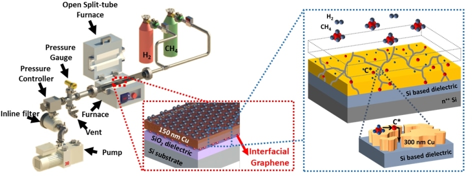
“This can be a game-changer for applications of graphene”, said Vikas Berry, Department Head of Chemical Engineering at University of Illinois at Chicago (UIC). Graphene is a two-dimensional network of sp2-hybridized carbon atoms with promise in nanoelectronics, optoelectronics, and photonics due its ultrafast carrier mobility, high mechanical strength, and high optical transparency. The current challenge in graphene electronics is graphene’s contamination-prone transfer from metal onto the desired substrate. This transfer-process introduces unwanted defects in graphene such as adsorption of polymeric impurities and surface corrugations.
The researchers at UIC and SunEdison Semiconductor in USA developed a process1-3 called ‘grain boundary-diffusion of carbon radicals’ for the transfer-free growth of graphene on effectively any semiconducting or insulating solid substrate. Here, methane (or other carbon sources) molecules are dissociated on metal deposited on the substrate in a vacuum and heated furnace. The carbon radicals produced from methane dissociation diffuses through the grain boundary of the metal and then crystallize to form graphene at the interface of metal and the underlying substrate. This growth strategy is suitable to produce large-scale graphene for industrial applications.
- MR Seacrist, V Berry, “Direct formation of graphene on semiconductor substrates”, US Patent 8,884,310
- MR Seacrist, V Berry, PT Nguyen, “Direct and sequential formation of monolayers of boron nitride and graphene on substrates”, US Patent 9,029,228
- P Nguyen, SK Behura, MR Seacrist, V Berry, “Carbon-Radical’s Intra-Grain-Diffusion for Wafer-Scale, Direct Growth of Graphene on Silicon-Based Dielectrics”, ACS applied materials & interface (DOI: 10.1021/acsami.8b07655) 2018