Jun 12 2008
A new way of bending X-ray beams developed by MIT researchers could lead to greatly improved space telescopes, as well as new tools for biology and for the manufacture of semiconductor chips.
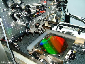 Gratings used to manipulate X-rays for future space telescopes and other applications, like tiny miniaturized venetian blinds, were created using this interference lithography patterning tool, called the nanoruler, developed at MIT's Space Nanotechnology Laboratory. The colorful, diffracting wafer at center has a diameter of 12 inches. Photo / Ralf Heilmann
X-rays from space provide astronomers with important information about the most exotic events and objects in our universe, such as dark energy, black holes and neutron stars. But X-rays are notoriously difficult to collect and many interesting cosmic sources are faint, which makes collecting these high-energy rays difficult and time-consuming, even with telescopes on satellites far above our X-ray-absorbing atmosphere.
Now a group of researchers from MIT has fabricated a new, highly efficient nanoscale Venetian-blind-like device that contains thousands of ultrasmooth mirror slats per millimeter for use in future improved space-based X-ray telescopes. The so-called Critical-Angle Transmission (CAT) gratings feature dense arrays of tens-of-nanometer-thin, freely suspended silicon structures that serve as efficient mirrors for the reflection and diffraction of nanometer-wavelength light--otherwise known as X-rays.
New instrument designs based on these gratings could also lead to advances in fields beyond astrophysics, from plasma physics to the life and environmental sciences, as well as in extreme ultraviolet lithography, a technology of interest to the semiconductor industry. The concept behind CAT gratings might also open new avenues for devices in neutron optics and for the diffraction of electrons, atoms and molecules.
Based on an invention by Ralf Heilmann and Mark Schattenburg of the Space Nanotechnology Laboratory (SNL) at the MIT Kavli Institute of Astrophysics and Space Research, the daunting fabrication challenges were overcome by graduate student Minseung Ahn of the Department of Mechanical Engineering at MIT in a yearlong effort, with the help of financial support from NASA and a Samsung Fellowship.
Motivated by technology goals for NASA's next-generation X-ray telescope, called Constellation-X, the new devices promise to improve more than five-fold upon the efficiency of the transmission gratings on board NASA's Chandra X-Ray Observatory (launched in 1999), which were also built at the Space Nanotechnology Lab. The reason for this improvement lies in the fact that in the new design, X-rays are reflected very efficiently at very shallow angles--akin to skipping stones on water--from the sub-nanometer-smooth sidewalls of the silicon slats, through the spaces between the slats. Also, in the earlier version the X-rays had to pass through a supporting substrate of polyimide, which absorbed many of the rays and reduced the grating's efficiency.
The silicon slats--as thin as 35 nanometers, which is comparable to the smallest feature sizes still under development in commercial computer chip manufacturing--are parallel to each other and separated by as little as about 150 nanometers. The slats have to extend many micrometers in the remaining two dimensions. "Imagine a thin, 40-foot-long, 8-foot-tall mirror, with surface roughness below a tenth of a millimeter," says Heilmann. "Then put tens of thousands of these mirrors next to each other, each spaced precisely an inch from the next. Now shrink the whole assembly--including the roughness--down by a factor of a million, and you have a good CAT grating."
Recent X-ray test results from a prototype device, obtained with the help of Eric Gullikson of Lawrence Berkeley National Laboratory, confirmed that it met theoretical expectations. The results of this work will be published in Optics Express (Vol. 16, No. 12) on June 9. They were also presented at the 52nd Intl. Conference on Electron, Ion and Photon Beam Technology and Nanofabrication in Portland, Ore., on May 28, and will be presented again at the SPIE Conference on Astronomical Telescopes and Instrumentation in Marseille, France, on June 23.